Machining method of printed circuit board (PCB) of step blind slot

A technology of PCB board and processing method, which is applied in the processing field of stepped blind groove PCB board, can solve the problems of abnormal gap, large labor cost, and insignificant glue resistance effect, and achieves good glue resistance effect and reduces abnormal gap effect.

Active Publication Date: 2012-11-07
GCI SCI & TECH
View PDF8 Cites 22 Cited by
  • Summary
  • Abstract
  • Description
  • Claims
  • Application Information

AI Technical Summary

Problems solved by technology

[0004] However, the step blind groove PCB board processed by the prior art has the problem that the glue resistance effect is not obvious, and the processed step blind groove will produce the problem of abnormal gap
The reason is that the thickness of the silicone gasket used for glue resistance cannot be exactly the same as the depth of the step blind groove. When the thickness of the silicone gasket is smaller than the depth of the step blind groove, it cannot achieve a good glue resistance effect during lamination, especially when using During the production of ordinary FR-4 (FR, flame retarded, flame retardant) prepregs with normal fluidity, a large amount of overflow glue will appear at the bottom of the stepped blind groove, while there are fewer manufacturers of prepregs with no fluidity or low fluidity, and the cost is higher; When the thickness of the silicone gasket is greater than the depth of the stepped blind groove, the silicone gasket is deformed under pressure during lamination, which will squeeze the silicone gasket from the edge of the stepped blind groove into the inner wall of the stepped blind groove, resulting in If the gap is abnormal, it will take a lot of manpower to repair it in the subsequent processing, and it may cause the PCB board to be scrapped during processing

Method used


Image

  • Machining method of printed circuit board (PCB) of step blind slot
  • Machining method of printed circuit board (PCB) of step blind slot
  • Machining method of printed circuit board (PCB) of step blind slot

Examples


Embodiment Construction

[0019] The following will clearly and completely describe the technical solutions in the embodiments of the present invention with reference to the accompanying drawings in the embodiments of the present invention. Obviously, the described embodiments are only some, not all, embodiments of the present invention. Based on the embodiments of the present invention, all other embodiments obtained by persons of ordinary skill in the art without creative efforts fall within the protection scope of the present invention.

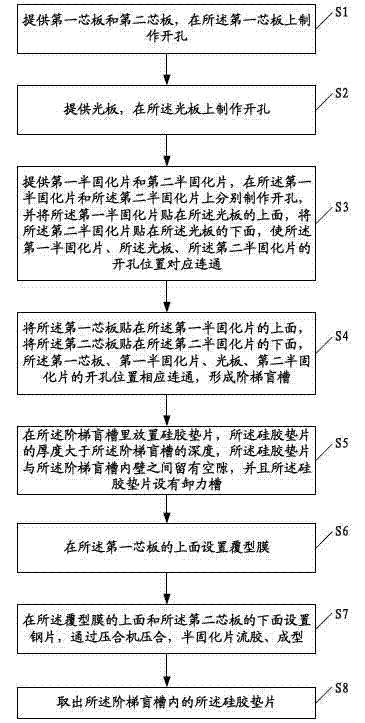
[0020] see figure 1 , is a schematic flowchart of an embodiment of a method for processing a stepped blind slot PCB provided by the present invention.

[0021] A method for processing a stepped blind groove PCB board provided in this embodiment includes:

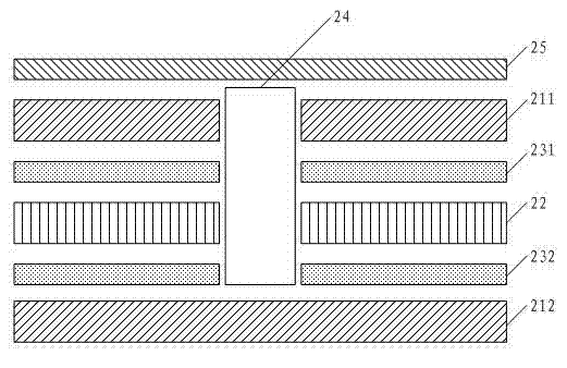
[0022] S1, providing a first core board and a second core board, and making holes on the first core board.

[0023] The first core board and the second core board provided can use common copper-clad core boards...


PUM


Abstract

The invention discloses a machining method of a printed circuit board (PCB) of a step blind slot. The method includes that a first core board and a second core board are provided, and holes are arranged on the first core plate; a light panel is provided and holes are arranged on the light panel; a first semi-curing plate and a second semi-curing plate are provided, holes are arranged on the semi-curing plates, and the first semi-curing plate and the second semi-curing plate are attached to the upper surface and the lower surface of the light panel respectively; the core plates are arranged on the outer lateral sides of the semi-curing plates, and the holes of the first core plate, the first semi-curing plate, the light panel and the second semi-curing plate form the step blind slot; a silica gel gasket is placed in the step blind slot, the thickness of the silica gel gasket is larger than the depth of the step blind slot, a gap is reserved between the silica gel gasket and an inner wall of the step blind slot, and the silica gel gasket is provided with a relief groove; a film is arranged on the upper face of the first core plate; a steel plate is arranged on the upper face and the lower face of a lamination and pressed through a press machine, glue of the semi-curing plates flows, and the semi-curing plates are molded; and the silica gel gasket in the step blind slot is taken out. By means of an embodiment of the machining method, glue blocking effect is good and seam abnormality of the blind slot is effective reduced.

Description

technical field [0001] The invention relates to the field of production and processing of printed circuit boards, in particular to a method for processing a stepped blind groove PCB board. Background technique [0002] For SMT needs, customers often have stepped blind slot design on PCB (PCB, Printed Circuit Board, printed circuit board), and have strict requirements on the quality of stepped blind slot. [0003] The existing lamination technology of stepped blind groove PCB boards mainly adopts no-flow type or low-flow type prepreg to produce, and fills the stepped blind groove with silicone gaskets that act as glue resistance. For example, Dongguan Shengyi Electronics Co., Ltd.'s application number is 200810142379.4 for the invention patent "Processing Method of Ladder PCB Board". [0004] However, the PCB with stepped blind slots processed in the prior art has the problem that the glue-repelling effect is not obvious, and the processed blind stepped slots have the proble...

Claims


Application Information

Patent Timeline
Patent Type & Authority Applications(China)
IPC IPC(8): H05K3/00
Inventor 张良昌尹益华
Owner GCI SCI & TECH
Why Eureka
Try Eureka