Integrated circuit or discrete component flat bump package technics and its package structure

A flat bump type, discrete component technology, applied in electrical components, circuits, electrical solid devices, etc., can solve problems such as ability to affect solderability, poor contact, contact cracking, etc., to achieve product quality assurance, reliability assurance , to ensure the effect of stability

Active Publication Date: 2006-02-22
长电科技管理有限公司
View PDF0 Cites 1 Cited by
  • Summary
  • Abstract
  • Description
  • Claims
  • Application Information

AI Technical Summary

Problems solved by technology

[0004] 2. Chemical adhesive film: due to the penetrating etching method, it will cause overflow during the encapsulation process
[0005] 3. Pollution: Because of the use of chemical tape, the adhesive of the film is easily vaporized due to high temperature in various high-temperature processes, and indirectly pollutes or covers the surface of the chip's pressing area and the wiring area, often causing wiring Instability of ability
[0009] B. Because of the fear of a large amount of rework after flashing, I dare not use a large encapsulation pressure. As a result, the plastic encapsulation compound is loose, the water absorption rate is increased, and the density is reduced, which seriously increases the production cost and yield cost;
[0010] C. The part of the bottom output pin of the four-sided surface mount type package is at the same height as the surface of the plastic package or even recessed. During the surface mount process, there will be a problem of poor contact due to poor coplanarity of the soles of the feet; at the same time, due to The outer pin is sunken in the plane of the plastic package, air will remain in the sunken during surface mount operation, and the contact will be broken after the high-temperature air expands;
[0011] D. Because the output pin and the plastic package are on the same plane or even recessed, it is easy to cause the solder paste on the surface of the protruding pin to connect to each other and short circuit during the surface mount process;
[0012] E. In principle, the inner pin of the wiring is silver-plated. However, the bonding ability between the silver layer and the molding compound is not good, and it is easy to cause delamination between the molding compound and the silver layer;
[0013] F. In principle, the outer pins of the electrical output are made of tin-lead, pure tin and other materials, and because the material itself is easy to oxidize, it will affect the ability of solderability, and the storage time is also short
[0014] G. Since the outer pins of the electrical output pins are made of tin-lead, pure tin and other materials in principle, and the melting point of tin is relatively low, so it is easy to cause tin oxidation or even damage due to the heat generated by the friction of the cutting knife during the cutting process. Melting, which greatly affects the solderability of the output pin and the stability of electrical transmission
[0015] 6. Heat dissipation and conductivity: The lead frame of the four-sided surface mount package is made of fully etched copper alloy, and its conductivity / heat dissipation capacity is only about 65%. If pure copper is used, its conductivity / heat dissipation capacity At least up to 99%; but because the strength of pure copper is too soft, it is easy to be troubled by the lead frame being too soft and easily deformed during the production process

Method used


Image

  • Integrated circuit or discrete component flat bump package technics and its package structure
  • Integrated circuit or discrete component flat bump package technics and its package structure
  • Integrated circuit or discrete component flat bump package technics and its package structure

Examples


Embodiment Construction

[0055] The integrated circuit or discrete component planar bump type packaging process of the present invention consists of the following procedures:

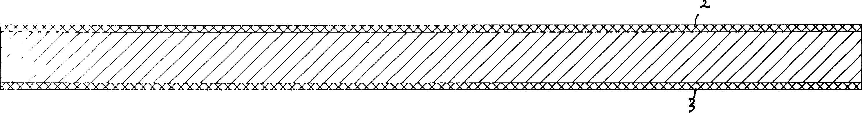
[0056] 1) Substrate - see figure 1 , take a piece of metal substrate 1 with an appropriate thickness. The material of the metal substrate 1 can be changed according to the functions and characteristics of the chip, for example: nickel-iron alloy, pure copper or copper alloy.

[0057] 2) Applied dry film - see figure 2 , affix dry film layers 2 and 3 on both sides of the metal substrate to protect the subsequent etching process.

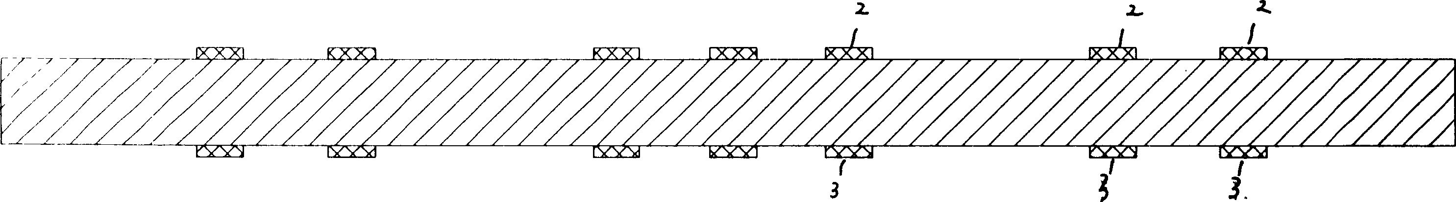
[0058] 3) Remove part of the dry film - see image 3 , correspondingly remove part of the dry film on both sides of the metal substrate 1, and prepare to form base islands and pins on the metal substrate 1, in order to expose the area on the substrate that needs to be plated with activating substances later,

[0059] 4) Plating activating substances - see Figure 4 , both sides of the base islan...


PUM


Abstract

The invention relates to a plane point-protruded type packaging process and its structure of integrated circuit or discrete component, comprising following steps: pasting dry films (2, 3) on the two surfaces of a metallic base plate (1) while removing some dry films relatively; plating active compound and metallic layer on the area of base plate for forming base island and pins; removing the left dry film on the front of base plate; half etching to form a depressed half etched region (1, 3), base island 1.1 and pin 1.2; removing the dry film left on the back of base plate; planting chip (9) into the front metal layer of base island, tie metallic thread (10), packaging plastic packaging body (11), front printing (12), and etching again on the left metal 1.4 of half etched region (1.3); pasting film (13) on the face of plastic packaging body, and slicing. Said invention has strong welding property, better quantity, low cost, good adaptability, reflex able arrangement of chips, while avoiding the problem of infiltration of plastic packaging material.

Description

Technical field: [0001] The invention relates to a planar bump packaging process for integrated circuits or discrete components and a packaging structure thereof. It belongs to the technical field of packaging of integrated circuits or discrete components. Background technique: [0002] The traditional ultra-thin leadless packaging process and packaging structure of integrated circuits or discrete components, the package type is four-sided leadless surface mount package, and the array assembly is cut into a single unit. Its substrate type is lead frame type. It mainly has the following deficiencies: [0003] 1. Lead frame: The lead frame is made by penetrating etching. [0004] 2. Chemical adhesive film: because of the penetrating etching method, it will cause overflow during the encapsulation process. [0005] 3. Pollution: Because of the use of chemical tape, the adhesive of the film is easily vaporized due to high temperature in various high-temperature processes, and...

Claims


Application Information

Patent Timeline
Patent Type & Authority Applications(China)
IPC IPC(8): H01L21/50H01L21/60H01L23/48H01L23/31
CPCH01L2224/32245H01L24/97H01L2224/48091H01L2224/45124H01L2224/83192H01L2224/73265H01L2224/48247H01L2924/01047H01L2224/48465H01L2224/45144H01L2224/45147H01L2224/92247H01L2224/29339H01L2224/45139H01L2224/97H01L2924/01322H01L2924/14H01L2924/00014H01L2924/00
Inventor 王新潮于燮康梁志忠谢洁人陶玉娟周正伟
Owner 长电科技管理有限公司
Why Eureka
Try Eureka