3D IC testing apparatus

A technology of testing equipment and equipment, applied in electronic circuit testing, automated testing systems, semiconductor/solid-state device testing/measurement, etc., and can solve problems such as defects caused by operational changes

Active Publication Date: 2012-11-14
TAIWAN SEMICON MFG CO LTD
View PDF5 Cites 20 Cited by
  • Summary
  • Abstract
  • Description
  • Claims
  • Application Information

AI Technical Summary

Problems solved by technology

When TSVs are formed before the different layers are stacked together, defec

Method used


Image

  • 3D IC testing apparatus
  • 3D IC testing apparatus
  • 3D IC testing apparatus

Examples


Embodiment Construction

[0030] The making and using of various embodiments of the invention are discussed in detail below. It should be appreciated, however, that the present invention provides many applicable concepts that can be implemented in a wide variety of specific contexts. The specific embodiments discussed are merely illustrative of specific ways to make and use the invention, and do not limit the scope of the invention.

[0031] The present invention will be described using a test scheme for through-silicon via (TSV) chains according to preferred embodiments in a specific context. However, the present invention is also applied to various TSV electrical characteristic tests.

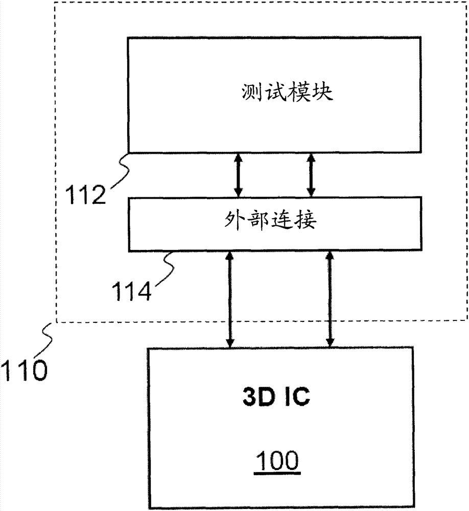
[0032] first reference figure 1 , shows a block diagram of a three-dimensional (3D) integrated circuit (IC) testing device according to an embodiment. When the 3D IC 100 operates in the test mode, the 3D IC test device 110 is connected with the 3D IC 100 through a plurality of test channels, such as test probes. T...


PUM


Abstract

A three dimensional (3D) integrated circuit (IC) testing apparatus comprises a plurality of connection devices. When a device under test (DUT) (such as an interposer or a 3D IC) formed by a plurality of 3D dies operates in a testing mode, the 3D IC testing apparatus is coupled to the DUT via a variety of interface channels (such as probes). The connection devices and a variety of through silicon vias (TSVs) in the DUT form a TSV chain so that electrical characteristics of the variety of TSVs can be tested all at once.

Description

technical field [0001] The invention relates to the field of semiconductors, and more specifically, to a 3D IC testing device. Background technique [0002] With the development of semiconductor technology, three-dimensional (3D) integrated circuits (ICs) have become an effective option for further reducing the physical size of semiconductor chips. In semiconductor chip-based 3D ICs, active circuits are fabricated on separate wafers and each wafer die is stacked on top of another wafer die using pick-and-place techniques. on top. Higher densities can be achieved by using 3D ICs. In addition, 3D ICs enable smaller form factors, cost-effectiveness, enhanced performance, and lower power consumption. [0003] In the development process of 3D IC, an intermediate stage called 2.5D IC was produced. In a 2.5D IC, there may be multiple dies including active circuitry and multiple interposers including through silicon vias (TSVs). Unlike 3D ICs, in 2.5D ICs various dies including...

Claims


Application Information

Patent Timeline
IPC IPC(8): G01R31/28G01R1/073
CPCG01R1/07378Y02P80/30G01R31/2834G01R31/2884G01R31/2886H01L22/14
Inventor 王敏哲陈致嘉林鸿志彭经能陈颢
Owner TAIWAN SEMICON MFG CO LTD
Why Eureka
Try Eureka