A double-sided microlens array and its manufacturing method
A technology of microlens array and manufacturing method, which is applied in the direction of lens, microlithography exposure equipment, photoplate making process exposure device, etc., can solve the problems that the effective value cannot be obtained, the light cannot be effectively gathered, etc., and the angle of view can be increased Range, the effect of shortening the focal length
- Summary
- Abstract
- Description
- Claims
- Application Information
AI Technical Summary
Problems solved by technology
Method used
Image
Examples
Embodiment 1
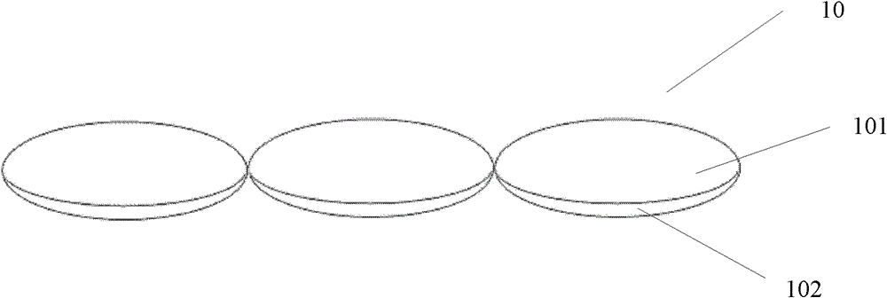
[0059] The invention proposes a double-sided microlens array to increase the viewing angle of the microlens array and shorten the focal length of the microlens array. Such as figure 2 As shown, the double-sided microlens array can specifically include: an array of double-sided microlenses 10, wherein each double-sided microlens 10 in the array includes an upper layer of micro-convex lenses 101 and a lower layer of micro-convex lenses 102; each double-sided micro-lens In 10, the upper-layer micro-convex lenses 101 and the lower-layer micro-convex lenses 102 are arranged in a one-to-one correspondence with the center, and the corresponding upper-layer micro-convex lenses 101 and the lower layer of micro-convex lenses 102 are bonded together.
[0060] In the embodiment of the present invention, by setting each microlens in the microlens array as a double-sided microlens including an upper layer of micro-convex lenses and a lower layer of micro-convex lenses, the incident light can...
Embodiment 2
[0068] In the embodiment of the present invention, the manufacturing method of the above-mentioned double-sided microlens array is shown, as Figure 7 As shown, the method may include the following processing steps:
[0069] Step 101, providing a substrate;
[0070] Step 102, etching a cavity array having the same width as the double-sided microlens on the substrate;
[0071] For simplicity, only one microlens in the double-sided microlens array is taken as an example, such as Figure 8 As shown, 801 is a substrate, usually silicon; 802 is a cavity with a uniform shape formed by etching on a silicon substrate;
[0072] Step 103, in each cavity, form the concave surface required for making the micro-convex lens in the lower layer by anisotropic etching; the concave surface is as follows Figure 8 as shown in 803;
[0073] Step 104, injecting the second material forming the lower layer of micro-convex lenses and the first material forming the upper layer of micro-convex lens...
PUM
 Abstract
Description
Claims
Application Information
 - R&D
- Intellectual Property
- Life Sciences
- Materials
- Tech Scout
- Unparalleled Data Quality
- Higher Quality Content
- 60% Fewer Hallucinations
Browse by: Latest US Patents, China's latest patents, Technical Efficacy Thesaurus, Application Domain, Technology Topic, Popular Technical Reports.
© 2025 PatSnap. All rights reserved.Legal|Privacy policy|Modern Slavery Act Transparency Statement|Sitemap|About US| Contact US: help@patsnap.com


