Supercharge Your Innovation With Domain-Expert AI Agents!

Semiconductor light source module, production method and substrate structure thereof

A technology of a light source module and a manufacturing method, which is applied to semiconductor devices, electrical components, circuits, etc., can solve the problems that the uniformity of the substrate structure is difficult to control, occupies the space of the substrate structure, and the volume of components cannot be reduced.

Inactive Publication Date: 2012-11-21
ADVANCED SEMICON ENG INC
View PDF3 Cites 3 Cited by
  • Summary
  • Abstract
  • Description
  • Claims
  • Application Information

AI Technical Summary

Problems solved by technology

However, the through-holes will occupy a certain space in the substrate structure, so the more through-holes will make the volume of the device unable to be reduced and the uniformity of the substrate structure in the fabrication is also difficult to control

Method used


Image

  • Semiconductor light source module, production method and substrate structure thereof
  • Semiconductor light source module, production method and substrate structure thereof
  • Semiconductor light source module, production method and substrate structure thereof

Examples


Embodiment Construction

[0036] The following examples are provided for detailed description, and the examples are only used as examples for illustration and will not limit the scope of protection of the present invention. In addition, some components are omitted from the drawings in the embodiments to clearly show the technical characteristics of the present invention.

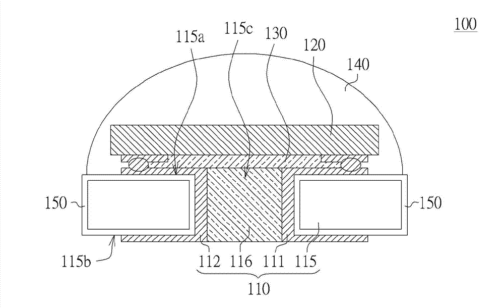
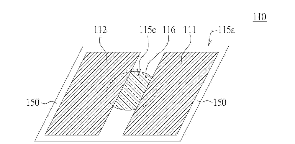
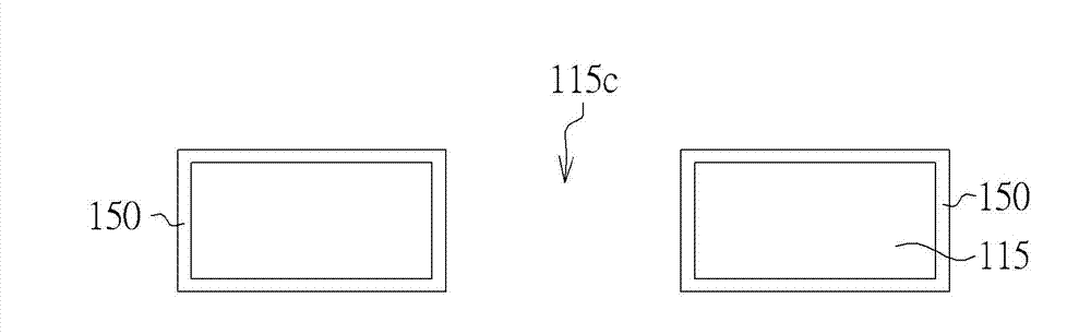
[0037] Please refer to figure 1 , which shows a schematic cross-sectional view of the semiconductor light source module 100 . The semiconductor light source module 100 mainly includes a substrate structure 110 and a light emitting diode (LED) 120 . The LED 120 is disposed on the substrate structure 110 . The light-emitting diode 120 is used to emit light, and its material is, for example, aluminum gallium arsenide (AlGaAs), aluminum gallium phosphide (AlGaP), aluminum indium gallium phosphide (AlGaInP), gallium arsenide phosphide (GaAsP), gallium phosphide (GaP ), gallium nitride (GaN), indium gallium nitride (InGaN), or aluminum ...


PUM


Abstract

The invention relates to a semiconductor light source module, a production method and a substrate structure of the semiconductor light source module. The semiconductor light source module comprises a substrate structure and a light emitting diode. The substrate structure comprises a base material, a first conductive trace, a second conductive trace and a filling material. The base material is provided with a first surface, a second surface and a through opening. The first surface is opposite to the second surface. The first conductive trace extends to the second surface from the first surface through the through opening. The second conductive trace extends to the second surface from the first surface through the through opening. The filling material is filled in the through opening. The light emitting diode is arranged on the first surface and is electrically connected with the first and second conductive traces. The projecting range of the light emitting diode covers the through opening.

Description

technical field [0001] The present invention relates to a semiconductor module, its manufacturing method and its substrate structure, and in particular to a semiconductor light source module, its manufacturing method and its substrate structure. Background technique [0002] With the development of semiconductor technology, various semiconductor light sources are constantly being introduced. For example, a light-emitting diode produces electroluminescence through the combination of electrons and holes within it. The wavelength of the light of the light-emitting diode is related to the type of semiconductor material and the dopant used. Light-emitting diodes have the advantages of high efficiency, long life, not easy to break, high switching speed, high reliability, etc., so that light-emitting diodes have been widely used in various electronic products. [0003] Light-emitting diodes are made into individual grains using semiconductor equipment. In order to allow the ligh...

Claims


Application Information

Patent Timeline
IPC IPC(8): H01L33/00H01L33/48H01L33/62
Inventor 黄彦良蔡宗岳赖逸少
Owner ADVANCED SEMICON ENG INC
Features
  • R&D
  • Intellectual Property
  • Life Sciences
  • Materials
  • Tech Scout
  • Unparalleled Data Quality
  • Higher Quality Content
  • 60% Fewer Hallucinations
Learn More