Multilayer package substrate and package

A technology for packaging substrates and packages, which is applied to electrical components, electrical solid-state devices, semiconductor devices, etc., can solve the problems of reducing manufacturability, warping of packaging substrates, etc., and achieve the effect of improving electrical performance

Active Publication Date: 2015-10-07
JIANGNAN INST OF COMPUTING TECH
View PDF3 Cites 0 Cited by
  • Summary
  • Abstract
  • Description
  • Claims
  • Application Information

AI Technical Summary

Problems solved by technology

Unbalanced via distribution between upper build-up layer 1 and lower build-up layer 3 can easily lead to package substrate warping, thereby reducing manufacturability

Method used


Image

  • Multilayer package substrate and package
  • Multilayer package substrate and package
  • Multilayer package substrate and package

Examples


Embodiment Construction

[0024] In order to make the content of the present invention clearer and easier to understand, the content of the present invention will be described in detail below in conjunction with specific embodiments and accompanying drawings.

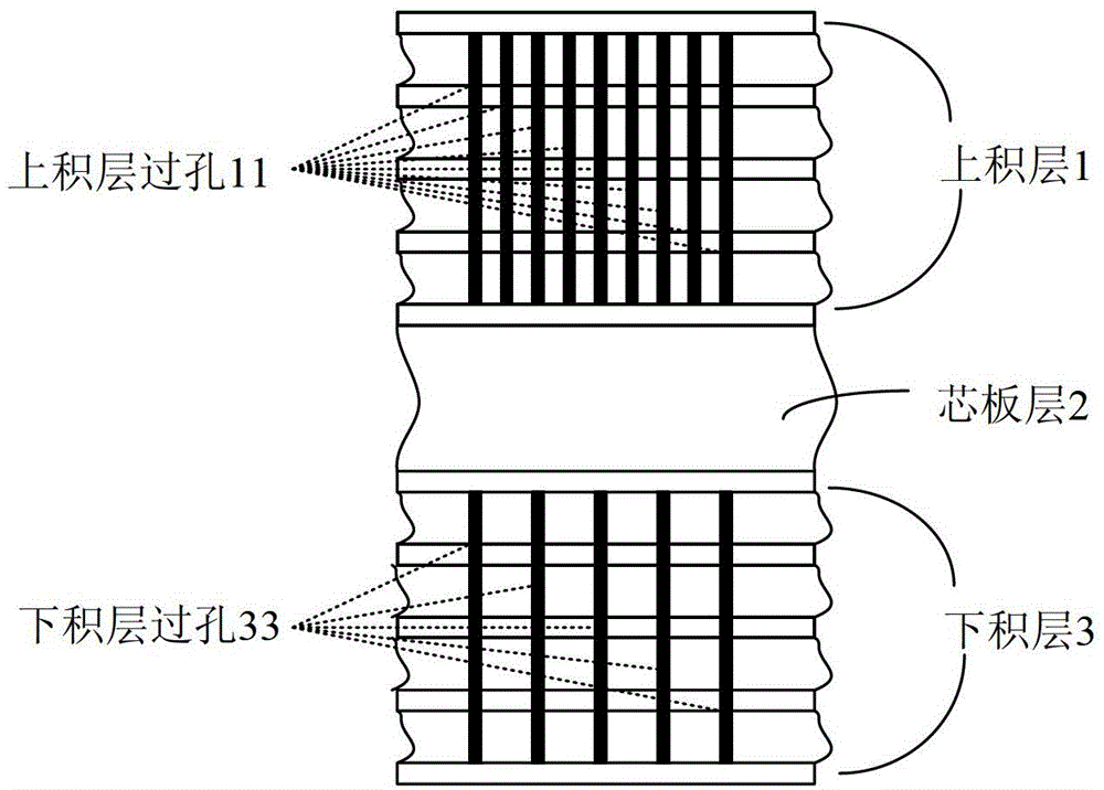
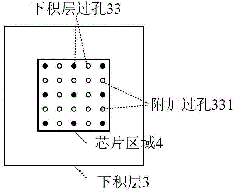
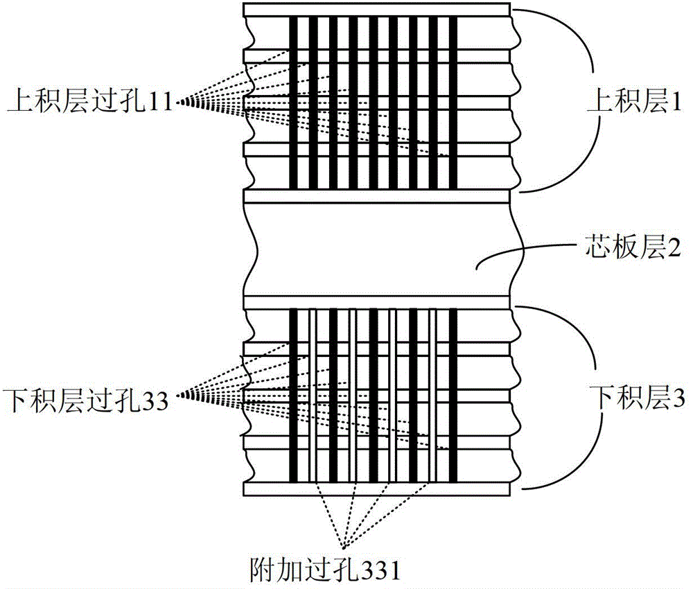
[0025] The pitch of the chip pins on the top layer of the multilayer packaging substrate is much smaller than that of the bottom layer of the packaging substrate, so the density of the via holes 11 in the upper buildup layer 1 of the multilayer packaging substrate is much greater than that of the lower buildup layer 3 . The density of the build-up vias 33 and the unbalanced via distribution between the upper build-up layer 1 and the lower build-up layer 3 easily lead to warping of the packaging substrate, thereby reducing the manufacturability of the high-density multilayer packaging substrate. Therefore, in the embodiment of the present invention, the chip area of ​​the lower build-up layer 3 of the multi-layer packaging substrate can be effecti...


PUM


Abstract

The invention provides a multilayer package substrate and a package member. The multilayer package substrate provided by the invention comprises an upper lamination layer, a core plate layer and a lower lamination layer, all of which are stacked in sequence, wherein a chip area of the upper lamination layer is provided with a plurality of upper lamination layer via holes; a chip area of the lower lamination layer is provided with a plurality of lower lamination layer via holes; and the plurality of lower lamination layer via holes in the chip area of the lower lamination layer comprise additional via holes, so that the density of the lower lamination layer via holes in the chip area of the lower lamination layer approaches the density of the upper lamination layer via holes in the chip area of the upper lamination area. Accordingly, the density of the via holes in the chip area between the upper lamination layer and the lower lamination layer inside the package substrate can be balanced, the package substrate can be prevented from warping, and the manufacturability of the multilayer package substrate is improved.

Description

technical field [0001] The invention relates to semiconductor packaging technology; more specifically, the invention relates to a multilayer packaging substrate and a package using the multilayer packaging substrate. Background technique [0002] Packaging is an important part of electronic components. With the increasing integration of electronic devices, the structure of packaging substrates (especially multi-layer packaging substrates) is becoming more and more complex, and accordingly the difficulty of its manufacture is also significantly increasing. At present, in the design of multilayer packaging substrates, the manufacturability of high-density multilayer packaging substrates is usually improved by adding stress relief points on the power ground plane layer. [0003] figure 1 A cross-sectional structure of a multilayer packaging substrate according to the prior art is schematically shown. [0004] Such as figure 1 As shown, the multilayer packaging substrate acc...

Claims


Application Information

Patent Timeline
Patent Type & Authority Patents(China)
IPC IPC(8): H01L23/522
Inventor 金利峰胡晋李川王玲秋贾福桢
Owner JIANGNAN INST OF COMPUTING TECH
Why Eureka
Try Eureka