Thin film transistor construction with large channel width and thin film transistor substrate circuit

A technology of thin film transistors and substrates, applied in circuits, electrical components, semiconductor devices, etc., can solve the problems of limited channel length and width changes, and the inability to improve the charging capacity of thin film transistors, etc.

Inactive Publication Date: 2012-11-28
TCL CHINA STAR OPTOELECTRONICS TECH CO LTD
View PDF4 Cites 12 Cited by
  • Summary
  • Abstract
  • Description
  • Claims
  • Application Information

AI Technical Summary

Problems solved by technology

[0012] The main purpose of the present invention is to provide a thin film transistor structure and a thin film transistor substrate circuit with a large channel width to solve the problem in the prior art that the charging capacity of the thin film transistor cannot be improved due to the limited change of the channel length and width of the thin film transistor

Method used


Image

  • Thin film transistor construction with large channel width and thin film transistor substrate circuit
  • Thin film transistor construction with large channel width and thin film transistor substrate circuit
  • Thin film transistor construction with large channel width and thin film transistor substrate circuit

Examples


Embodiment Construction

[0037] In order to make the above objects, features and advantages of the present invention more comprehensible, preferred embodiments of the present invention will be described in detail below together with the accompanying drawings. In order to make the above objects, features and advantages of the present invention more comprehensible, preferred embodiments of the present invention are exemplified below and described in detail in conjunction with the accompanying drawings. Furthermore, the directional terms mentioned in the present invention, such as "up", "down", "front", "rear", "left", "right", "inside", "outside", "side", etc., It is only for orientation with reference to the attached drawings. Therefore, the directional terms used are used to illustrate and understand the present invention, but not to limit the present invention.

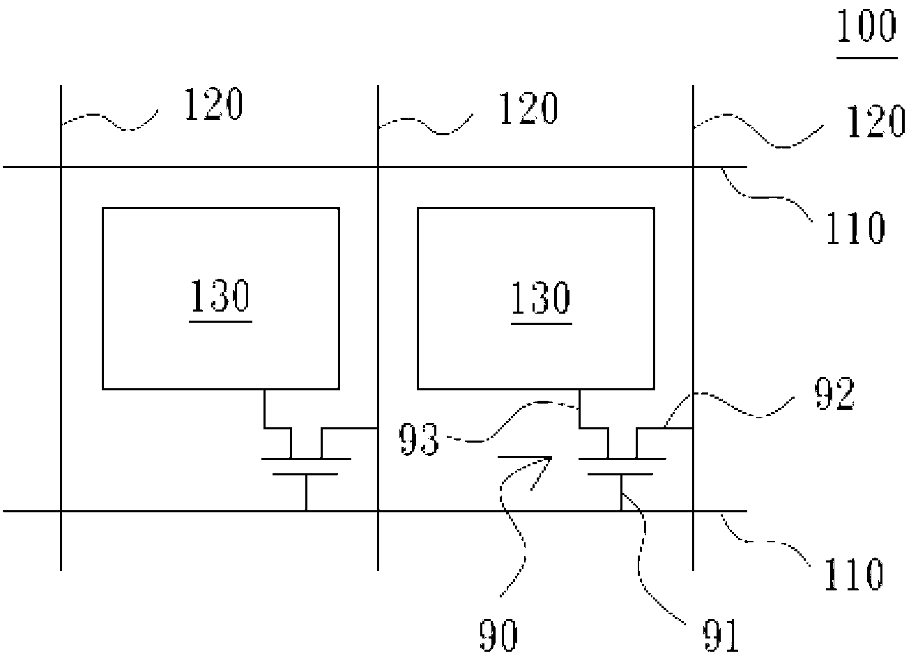
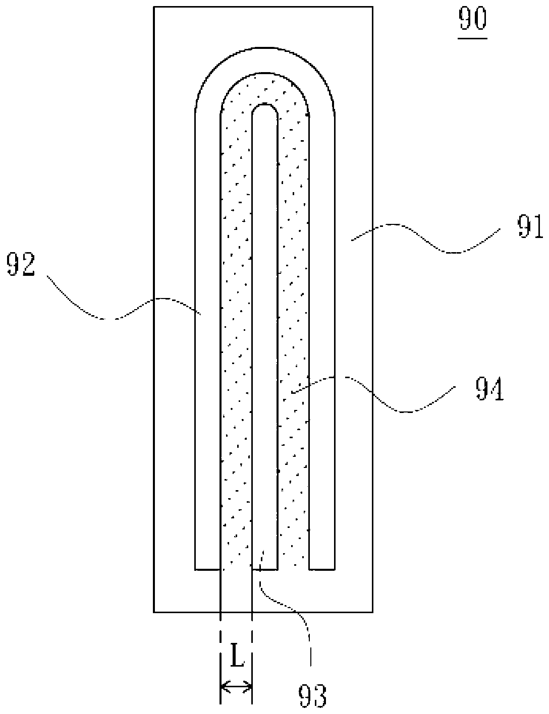
[0038] Please refer to image 3 as shown, image 3 is a partial schematic diagram of a thin film transistor (thin film transistor, TFT) ...


PUM

PropertyMeasurementUnit
areaaaaaaaaaaa
widthaaaaaaaaaa

Abstract

The invention discloses a thin film transistor construction with large channel width. The thin film transistor construction comprises a grid electrode, a source electrode and a drain electrode, wherein the source electrode and the drain electrode are helix and are symmetrical and corresponding to each other, and a double-helix configuration. In the thin film transistor construction, the source electrode and the drain electrode are designed into double-helix shape, the width of a channel between the source electrode and the drain electrode is increased, and the width to length ratio of the channel is increased so as to improve the charging capacity of the thin film transistor.

Description

【Technical field】 [0001] The invention relates to a thin film transistor structure and a thin film transistor substrate circuit with a large channel width, in particular to a thin film transistor structure and a thin film transistor substrate circuit of a liquid crystal display with a spiral source and drain. 【Background technique】 [0002] Thin film transistor (thin film transistor, TFT) technology is a large-scale semiconductor full integrated circuit manufacturing technology developed since the 1990s, and is the basis for the development of liquid crystal flat panel display (FPD). Liquid crystal display (LCD) has become a research hotspot and leading technology in the field of information display technology due to its lightness, portability, low power consumption and easy integration. It is currently mainly used in digital cameras, notebook computers, global navigation systems ( GPS), various monitors, etc. With the advent of the information society, the application fiel...

Claims


Application Information

Patent Timeline
Patent Type & Authority Applications(China)
IPC IPC(8): H01L29/417H01L29/78G02F1/1368
CPCH01L29/41733H01L29/78696H01L27/124
Inventor 康基善柯智胜何文超
Owner TCL CHINA STAR OPTOELECTRONICS TECH CO LTD
Why Eureka
Try Eureka