

Photoelectric conversion element and photoelectric converter
A technology for photoelectric conversion elements and charges, applied in electrical components, electric solid-state devices, circuits, etc., can solve the problems of image quality degradation, photodiodes are easily affected by optical noise, etc. The effect of suppressing false detections
- Summary
- Abstract
- Description
- Claims
- Application Information
AI Technical Summary
Problems solved by technology
Method used
Image

Examples
Deformed example
[0034] 6. Modification 4 (Example of deriving a signal from the lower side (n-type semiconductor layer))
Embodiment
[0036] structure
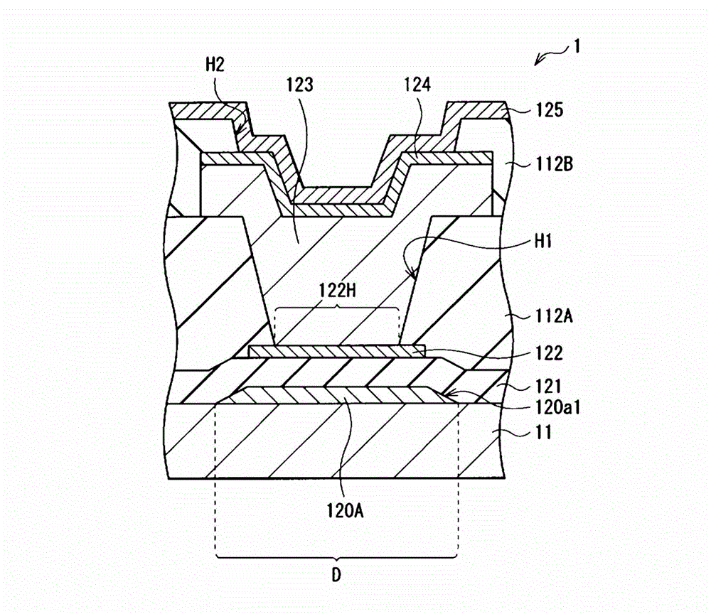
[0037] figure 1 A schematic structure of a photodiode (photodiode 1 ) according to an example of the present invention is shown. The photodiode 1 is a photoelectric conversion element for generating charges (photocharges) corresponding to the light amount of incident light (received light) and storing the generated charges inside it. The photodiode 1 is a PIN photodiode in which an i-type semiconductor layer (intrinsic semiconductor layer) is interposed between a p-type semiconductor layer and an n-type semiconductor layer.
[0038] The photodiode 1 has, for example, a p-type semiconductor layer 122 , an i-type semiconductor layer 123 , and an n-type semiconductor layer 124 stacked in this order from the side of a substrate 11 made of glass or other materials. More specifically, in the photodiode 1 , the p-type semiconductor layer 122 is provided in a selected region on the substrate 11 (more precisely, on an insulating film 121 described later). A first ...
Deformed example 1
[0071] Figure 7 A cross-sectional structure of a photodiode (photodiode 1A) of this modified example is shown. Like the photodiode 1 in the above-described embodiment, the photodiode 1A is also a PIN type photodiode, and has a p-type semiconductor layer 122C, an i-type semiconductor layer 123 and an n-type semiconductor layer 124 stacked in this order from the substrate 11 side. More specifically, the p-type semiconductor layer 122C is provided in selected regions on the substrate 11 . The first interlayer insulating film 112A is provided to have a contact hole H1 opposite to the p-type semiconductor layer 122C. The second interlayer insulating film 112B having the contact hole H2 is provided on the n-type semiconductor layer 124 and the first interlayer insulating film 112A. The upper electrode 125 is connected to the n-type semiconductor layer 124 through the contact hole H2. Furthermore, a light shielding layer 120B is provided between the p-type semiconductor layer 122...
PUM
 Abstract
Description
Claims
Application Information