Sub-wavelength electromagnetic diode

A diode and subwavelength technology, applied in the field of subwavelength electromagnetic diode devices, can solve the problems of application limitation and large volume of integrated circuits

Inactive Publication Date: 2012-11-28
TONGJI UNIV
View PDF3 Cites 0 Cited by
  • Summary
  • Abstract
  • Description
  • Claims
  • Application Information

AI Technical Summary

Problems solved by technology

[0003] The invention solves the problem that the existing diode device is large in size and has limitations on the application of integrated circuits, and discloses a design idea and means for realizing sub-wavelength electromagnetic diodes based on coupled resonance transmission

Method used


Image

  • Sub-wavelength electromagnetic diode
  • Sub-wavelength electromagnetic diode
  • Sub-wavelength electromagnetic diode

Examples


Embodiment 1

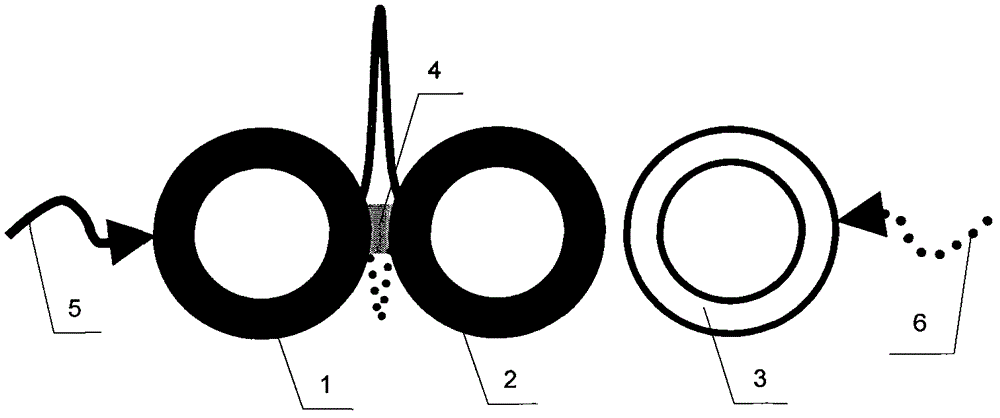
[0015] Please refer to the attached figure 1 , with figure 2 and attached image 3 .

[0016] The sub-wavelength electromagnetic diode involved in the present invention is composed of asymmetrically cascaded metal resonant units and parts with nonlinear response between some units. We give the design and experimental results of three resonant units in the microwave band, two of which are Components with nonlinear response between resonant units: metal resonant unit 1, metal resonant unit 2, patch circuit of metal resonant unit 3 and nonlinear component 4 between metal resonant unit 1 and metal resonant unit 2 (here, variable capacitor diode) and near-field feed probes 5, 6, see the appendix figure 1 . Specifically, metal resonance units 1 and 2 are 2.5mm×15.5mm, metal resonance unit 3 is 10.5×9.5mm, the distance between metal resonance units 1 and 2 is 0.8mm, and the distance between metal resonance units 2 and 3 is 0.5mm. The metal line width is 0.5mm .
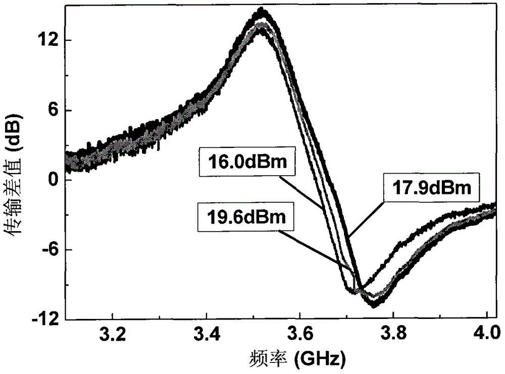
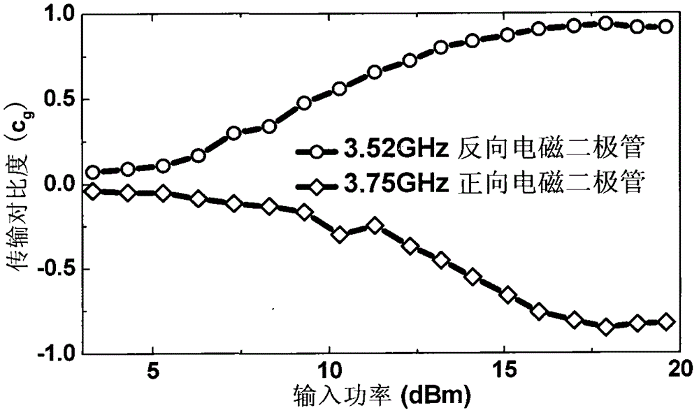
[0017] In thi...


PUM


Abstract

The invention discloses a sub-wavelength electromagnetic diode implemented on the basis of coupling resonance transmission. The sub-wavelength electromagnetic diode consists of three or more metal resonant units in asymmetric cascade connection, nonlinear response parts among part of the metal resonant units, and near-field feed-in and feed-out structures, wherein a plurality of metal resonant units are in cascade connection with one another in sequence, and the nonlinear response parts are required to be introduced among part of the metal resonant units; and the specific asymmetric introduction in the asymmetric cascade connection of the metal resonant units can be asymmetry caused by the nonlinear introduction in a symmetric cascade connection structure, or the asymmetry of a cascade connection structure. The sub-wavelength size of the electromagnetic diode is beneficial for miniaturization of integrated photon loops; low-power operation can be realized by using local field enhanced strong nonlinearity; two-frequency operation can be realized; and the sub-wavelength electromagnetic diode can be directly used as a component of an on-chip integrated photon loop.

Description

technical field [0001] The invention relates to a nonlinear control coupling resonant transmission device, in particular to a sub-wavelength electromagnetic diode device. Background technique [0002] Electromagnetic diode is a device that realizes unidirectional conduction of electromagnetic waves, and is one of the basic devices for constructing electromagnetic logic circuits. It has broad application prospects in the fields of communication and all-optical computing. At present, the relevant research at home and abroad mainly focuses on several aspects: the introduction of nonlinearity in photonic crystals, and the realization of diodes by using nonlinear modulation band-edge shift [Documents 1-2, M.Scalora, J.P.Dowling, C.M.Bowden, and M.J. Bloemer, "The photonic band edge optical diode," Journal of Applied Physics 76, 2023-2023 (1994); M.D. Tocci, M.J. Bloemer, M. Scalora, J.P. Dowling, and C.M. Bowden, "Thin-film nonlinear optical diode," Applied Physics Letters 66, ...

Claims


Application Information

Patent Timeline
IPC IPC(8): H01P1/32
Inventor 樊元成李宏强韩缙魏泽勇武超曹扬余兴
Owner TONGJI UNIV
Why Eureka
Try Eureka