
Semiconductor lighting device

A lighting device and semiconductor technology, applied in lighting devices, components of lighting devices, cooling/heating devices of lighting devices, etc., can solve problems that are not conducive to market competition, return to the factory for repair or discard, and do not consider the possibility of interoperability and other problems, to achieve the effect of solid semiconductor lighting devices and solve interchangeability problems

Active Publication Date: 2014-03-05
惠州雷士光电科技有限公司
View PDF8 Cites 0 Cited by
  • Summary
  • Abstract
  • Description
  • Claims
  • Application Information

AI Technical Summary

Problems solved by technology

However, due to the necessary design characteristics of LED light sources such as heat dissipation and driving power support, and the production companies have their own strengths, the possibility of intercommunication between companies and products of the same type is usually not considered, which will cause current problems. When the lighting product lamps of one company are not broken but the light source is damaged, it cannot be replaced by LED light sources of other companies, and vice versa. Therefore, unless the whole lamp is replaced, it will not be possible to continue to use the LED light source products of this company. This not only limits It is not conducive to market competition at the same time, it is even more uneconomical for consumers, and it is a waste
[0003] Secondly, because this kind of lighting products usually combine the light source and lamps with an integrated design, when the LED light source is damaged, ordinary consumers are faced with a large number of electronic components, and it is difficult for them to understand the cause of the damage, and it is impossible to replace or repair it by themselves. Instead, we can only ask the company to return to the factory for repair or discard, which not only increases the maintenance cost of consumers, but also increases the time cost, which brings a lot of inconvenience to consumers.

Method used


Image

  • Semiconductor lighting device
  • Semiconductor lighting device
  • Semiconductor lighting device

Examples


Embodiment Construction

[0022] The semiconductor lighting device of the present invention will be further described in detail below in conjunction with specific embodiments and accompanying drawings.

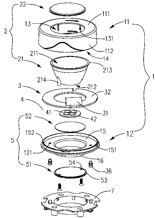
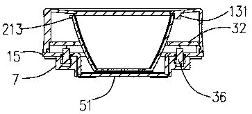
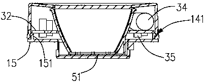
[0023] like Figure 1 to Figure 4 As shown, in a preferred embodiment, the semiconductor lighting device of the present invention mainly includes a housing 1 , an optical module 2 , a driving electronic module 3 , a light source module 4 and a heat treatment module 5 . Both ends of the housing 1 are open, and the shape can be generally cylindrical, square or triangular. The optical module 2, the driving electronic module 3, the light source module 4 and at least a part of the heat treatment module 5 are placed in the housing 1 to form a Integral lighting fixtures.

[0024] In this embodiment, the housing 1 includes an upper housing 11 and a lower housing 12 that are detachably connected together. The upper housing 11 is cylindrical, and includes a ring-shaped upper end surface 111 and a side wall 112...


PUM


Abstract

The invention relates to a shell. Openings are formed in two ends of the shell, and an optical module, a light source module, an electronic driving module and a heat treatment module are accommodated in the shell. The optical module is arranged on a center shaft in the shell; the top of the optical module is connected with the front end of the shell; the light source module is placed at the bottom of the optical module, and emits light towards the opening in the front end of the shell; the electronic driving module is hooped on the outer wall of the optical module; and the heat treatment module is arranged at the bottom of the light source module, and the opening in the rear end of the shell is closed by the heat treatment module. The optical module is used as an upright column of the semiconductor lighting device, and bears acting force from two ends of the shell and acting force from the heat treatment module, so that the semiconductor lighting device is firm, and the phenomenon that the semiconductor lighting device collapses due to over high pressure from the outer side and then is damaged is avoided.

Description

technical field [0001] The invention relates to a lighting device, in particular to a semiconductor lighting device. Background technique [0002] As a new type of light source, semiconductor light source (LED) is gradually replacing the position of traditional light source with its advantages of environmental protection, energy saving and longevity, and is widely used in various lighting fields. However, with the increasing number of LED lighting products on the market Rich, users gradually find several problems, first of all, lighting fixtures are usually composed of light sources and lamps, such as: LED downlights. However, due to the necessary design characteristics of LED light sources such as heat dissipation and driving power support, and the production companies have their own strengths, the possibility of intercommunication between companies and products of the same type is usually not considered, which will cause current problems. When the lighting product lamps o...

Claims


Application Information

Patent Timeline
Patent Type & Authority Patents(China)
IPC IPC(8): F21V19/00F21V17/10F21V29/00F21Y101/02F21V29/503F21V29/89
Inventor 田晓改王伟霞肖一胜郑子豪
Owner 惠州雷士光电科技有限公司
Learn More