Display device

A technology for display devices and shutter plates, which can be applied to microstructure devices, manufacturing microstructure devices, and microelectronic microstructure devices, etc. Effect

Inactive Publication Date: 2012-12-05
SNAPTRACK
View PDF7 Cites 5 Cited by
  • Summary
  • Abstract
  • Description
  • Claims
  • Application Information

AI Technical Summary

Problems solved by technology

[0008] However, when Figure 8A ~ Figure 8H When the shutter assembly is manufactured as shown, the unevenness of the film stress may occ

Method used


Image

  • Display device
  • Display device
  • Display device

Examples


Example

[0045] [first embodiment]

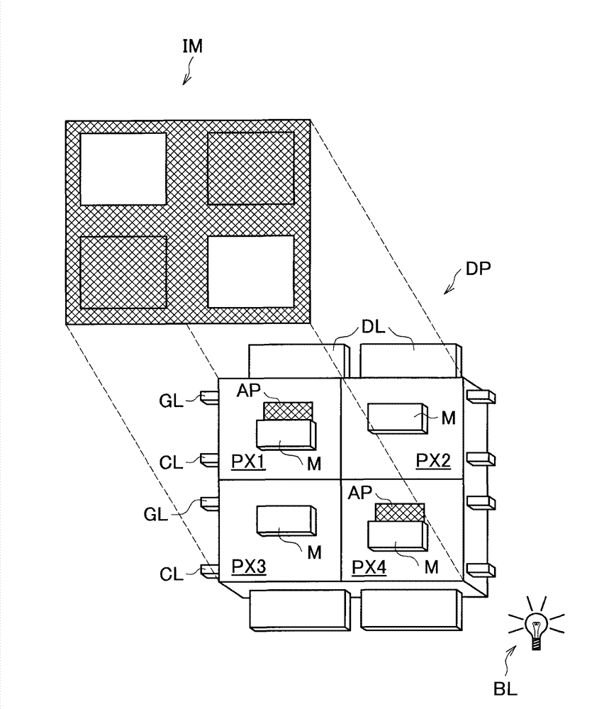
[0046] figure 1 It is a schematic diagram of the display device DP according to the first embodiment of the present invention. The display device DP has a shutter assembly M as a light modulator on each of a plurality of pixels arranged in a matrix. exist figure 1 In the schematic diagram of , the pixels PX1 and PX4 are in the open state and can transmit the light from the backlight BL of the hole AP to display white on the image IM. In addition, the pixels PX2 and PX3 are closed and block the transmission of light from the backlight BL, and display black on the image IM.

[0047]In addition, the display device DP includes a first substrate having a switching element on each of the plurality of pixels, and a second substrate disposed opposite to the first substrate. The shutter assembly M is disposed between the first substrate and the second substrate.

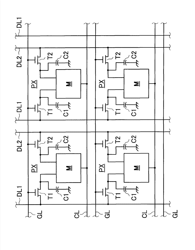
[0048] figure 2 It is a figure which shows the equivalent circuit of the 1st board|sub...

Example

[0075] [the second embodiment]

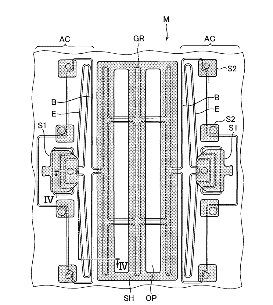
[0076] Next, a second embodiment of the present invention will be described. Image 6 is a diagram showing the cross section of the drive electrode E, the beam portion B, and the shutter SH in the second embodiment, and shows Figure 3A The portion from the drive electrode E to the shutter SH in the IV-IV section. The second embodiment differs from the first embodiment except that the region outside the drive electrode E, that is, the region inside the beam portion B is fully exposed through the half-tone mask in the first photolithography process. The situation is roughly the same.

[0077] Figure 7A ~ Figure 7C It is a figure explaining the state of manufacturing the shutter assembly M in 2nd Embodiment. First, if Figure 7A As shown, on the resist film RS1 used as a sacrificial layer, the portion where the drive electrode E and the beam portion B are formed is processed by full exposure in the same manner as the portion of the concave ...


PUM


Abstract

A display device includes: a plurality of pixels each having a shutter plate (SH) formed and an actuator portion (AC), wherein the actuator portion (AC) has a beam portion (B) connected to the shutter plate (SH), a drive electrode (E) causing the beam portion (B) to bend to drive the shutter plate (SH), a first supporting portion (S1) supporting the drive electrode (E) and fixed on a substrate (B1), and a second supporting portion supporting the beam portion (B) and fixed on the substrate, at least one of the first supporting portion and the second supporting portion has a planar portion (Sp), and a recessed portion (Sc) formed to be concaved from the planar portion (Sp) and connected to the substrate, and the recessed portion (Sc) has a vertically formed portion (Sv) formed to be inclined substantially vertically from the planar portion, and a portion (Sg) starting from the vertically formed portion (Sv) and formed such that the inclination of the portion becomes gentle toward the substrate (B).

Description

technical field [0001] The invention relates to a display device. Background technique [0002] A display is known in which a shutter (shutter) based on MEMS (Micro Electro Mechanical Systems) is arranged in each pixel of the display device, and an image is formed by opening and closing the shutter. [0003] As such a display device, for example, Japanese Patent Laid-Open No. 2008-197668 discloses a display using a MEMS-based mechanical light modulator and having a backlight. In addition, Japanese PCT Publication No. 2008-533510 also discloses a display device incorporating a MEMS-based light modulator, and the manufacturing method of the display device is described to be compatible with the manufacturing process of liquid crystal displays. the meaning of. [0004] Here, in a display device having a shutter assembly as an optical modulator in a plurality of pixels, the shutter assembly consists of a shutter plate formed in a plate shape and an actuator that drives the shut...

Claims


Application Information

Patent Timeline
IPC IPC(8): G02B26/02G09G3/34
CPCB81B2203/0307H02N1/006G02B26/02B81B2203/0376B81B2201/047B81C1/00103G02B26/00B32B3/00B81B3/0062B81B7/02G02B26/04G02F2203/12G09G3/34G09G5/10G09G2300/08
Inventor 木村泰一藤吉纯栗谷川武园田大介
Owner SNAPTRACK
Why Eureka
Try Eureka