High-temperature superconducting film magnet
A high-temperature superconducting thin film and superconducting thin film technology, which is applied in the field of superconducting engineering, can solve the problems that the volume cannot be small, the winding structure cannot be formed, and the strip cannot be bent at will, and the effect of high current density can be achieved.
- Summary
- Abstract
- Description
- Claims
- Application Information
AI Technical Summary
Problems solved by technology
Method used
Image
Examples
Embodiment 1
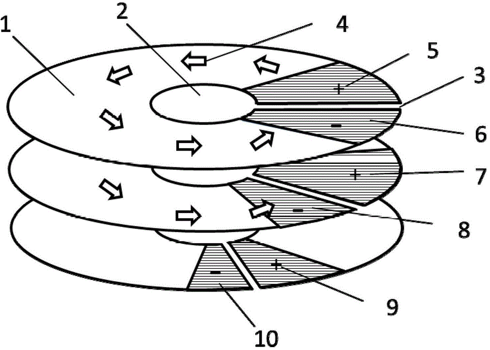
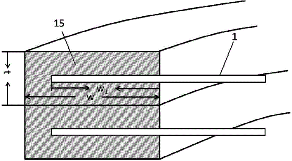
[0027] A high-temperature superconducting thin-film magnet, such as figure 1 As shown, the middle part of the superconducting thin film 1 is provided with a hole 2, and the superconducting thin film 1 is provided with a slit 3 along the radial direction, and the positive electrode 5 and the negative electrode 6 are respectively arranged on both sides of the slit 3, and the negative electrode 6 of the first layer of superconducting thin film is connected to The positive electrode 7 of the second layer of superconducting thin film, the negative electrode 8 of the second layer of superconducting thin film is connected to the positive electrode 9 of the third layer of superconducting thin film; The electrodes of each layer of superconducting thin film 1 are wrapped in a high-conductivity metal block 15, and the electrical conduction between superconducting thin films 1 is realized by welding between the metal blocks (such as image 3 and Figure 4 shown).
[0028] The contour di...
Embodiment 2
[0030] A high temperature superconducting thin film magnet, the superconducting thin film is provided with slits along the radial direction, positive poles and negative poles are respectively arranged on both sides of the slits, the positive poles are connected in sequence, and the negative poles are connected in sequence. When the electrodes pass through, a circular current is generated. The electrodes of each layer of superconducting film are wrapped in a high-conductivity metal block, and the electrical conduction between the superconducting films is realized through welding between the metal blocks.
Embodiment 3
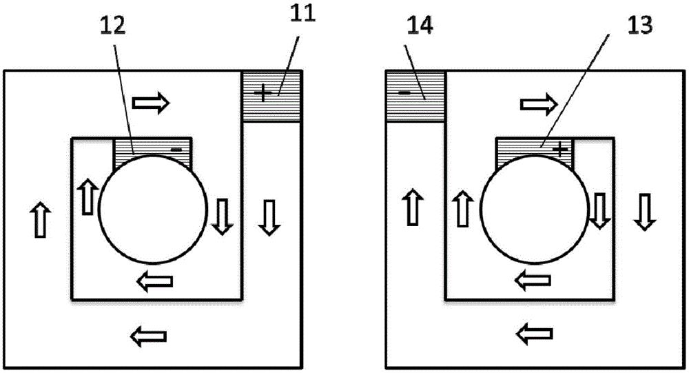
[0032] A high-temperature superconducting thin-film magnet, such as figure 2 As shown, the superconducting thin film 1 etches the helix, and electrodes are arranged on the innermost and outermost sides of the helix respectively. The three superconducting thin films 1 are connected in series, and the helical etching directions of the adjacent two superconducting thin films 1 are opposite. The superconducting thin film 1 is embedded in a high-conductivity metal block as a whole, and the metal block and the superconducting thin film 1 are engraved with the same texture. The current of the first layer of superconducting film flows in from the positive electrode 11 and flows out from the negative electrode 12 , while the negative electrode 12 is connected to the positive electrode 13 of the second layer of superconducting film, and the current flows out from the negative electrode 14 . The electrodes of each layer of superconducting film are wrapped in a high-conductivity metal bl...
PUM
| Property | Measurement | Unit |
|---|---|---|
| thickness | aaaaa | aaaaa |
Abstract
Description
Claims
Application Information


