Interlayer wiring of semiconductor device using carbon nanotube and method of manufacturing the same

a technology of carbon nanotubes and semiconductor devices, applied in the direction of semiconductor devices, semiconductor/solid-state device details, material nanotechnology, etc., can solve the problems of increasing the current density of metal wires while reducing the line width of metal wires, the degree of integration of semiconductor devices that use metal wires may reach limits in the near future, and the difficulty of increasing the density of carbon nanotubes, etc., to achieve the effect of increasing the current density and reducing the electrical resistan

Inactive Publication Date: 2008-09-04
SAMSUNG SDI CO LTD
View PDF1 Cites 31 Cited by
  • Summary
  • Abstract
  • Description
  • Claims
  • Application Information

AI Technical Summary

Benefits of technology

[0008]The present invention provides an interlayer wiring structure of a semiconductor device that can reduce electrical resistance and can increase current density, and a method of manufacturing the interlayer wiring structure.

Problems solved by technology

However, there is limitations for increasing the current density in the metal wires while reducing line width of the metal wires, even though the reduction of line width and the increase of current density are essential for the highly integrated semiconductor devices.
Therefore, it is expected that the degree of the integration of semiconductor devices that use metal wires may reach limits in the near future due to the reasons described above.
Although the wires of semiconductor devices can be replaced with carbon nanotubes, increasing density of the carbon nanotubes, however, is an issue, because the contemporary trend of the development of semiconductor devices would require more highly integrated semiconductor devices, and would require wires that could maintain higher current density without causing trouble.

Method used


Image

  • Interlayer wiring of semiconductor device using carbon nanotube and method of manufacturing the same
  • Interlayer wiring of semiconductor device using carbon nanotube and method of manufacturing the same
  • Interlayer wiring of semiconductor device using carbon nanotube and method of manufacturing the same

Examples


Embodiment Construction

[0020]The present invention will now be described more completely with reference to the accompanying drawings in which exemplary embodiments of the invention are shown. First, an interlayer wiring structure of a semiconductor device using carbon nanotubes will be described.

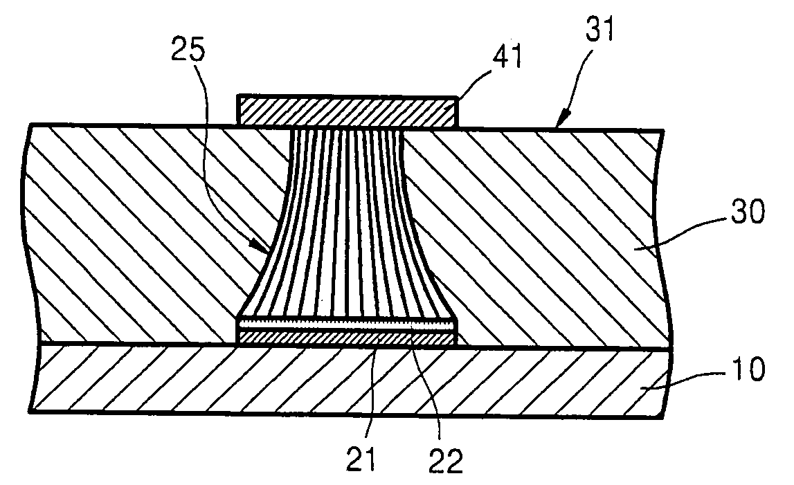
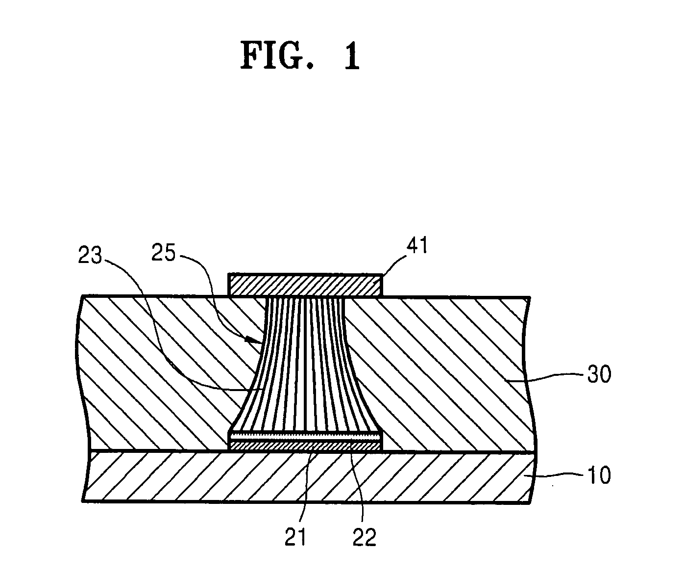
[0021]FIG. 1 is a cross-sectional view of an interlayer wiring structure of a semiconductor device constructed as an embodiment of the present invention. Lower electrode (or first electrode) 21 is formed on substrate 10. Catalyst layer 22 is formed on a surface of lower electrode 21 to grow carbon nanotubes from the surface. Carbon nanotube bundle 25 is formed between catalyst layer 22 and upper electrode (or second electrode) 41. Carbon nanotube bundle 25 is an interlayer wire that electrically connects lower electrode (first electrode) 21 to upper electrode (second electrode) 41.

[0022]Lower electrode 21, which is made of a conductive material, can be a part of an electrode pattern, or can be a part of a lower la...


PUM

PropertyMeasurementUnit
diameteraaaaaaaaaa
diameteraaaaaaaaaa
temperatureaaaaaaaaaa

Abstract

Provided is an interlayer wiring structure of a semiconductor device using carbon nanotubes, and a method of manufacturing the interlayer wiring structure. The interlayer wiring structure is a carbon nanotube bundle that connects a first electrode to a second electrode. The carbon nanotube bundle includes a plurality of carbon nanotubes grown from a catalyst layer that is formed on a first electrode. The carbon nanotube bundle is made in a manner that a portion of the carbon nanotube bundle close to the second electrode has higher density of carbon nanotubes than another portion of the carbon nanotube bundle close to the first electrode. The carbon nanotube bundle is surrounded by an interlayer dielectric. In one embodiment of a method of manufacturing the carbon nanotube interlayer wire, liquid droplets are distributed between the carbon nanotubes to induce surface tension between the carbon nanotubes. The surface tension makes the carbon nanotube bundle maintain higher density of carbon nanotubes in a portion close to the second electrode.

Description

CLAIM OF PRIORITY[0001]This application makes reference to, incorporates the same herein, and claims all benefits accruing under 35 U.S.C. §119 from an application for INTERLAYER WIRING OF SEMICONDUCTOR DEVICE USING CARBON NANOTUBE AND MANUFACTURING PROCESS OF THE SAME earlier filed in the Korean Intellectual Property Office on the 4 of Jul. 2006 and there duly assigned Serial No. 10-2006-0062412.BACKGROUND OF THE INVENTION[0002]1. Field of the Invention[0003]The present invention relates to an interlayer wiring of a semiconductor device and a method of manufacturing the same, and more particularly, to an interlayer wiring of a semiconductor device that uses carbon nanotubes to reduce electrical resistance and to increase current density, and to a method of manufacturing the interlayer wiring, which includes a process of forming a plurality of highly densified carbon nanotubes.[0004]2. Description of the Related Art[0005]Semiconductor devices, in particularly semiconductor memories,...

Claims


Application Information

Patent Timeline
Patent Type & Authority Applications(United States)
IPC IPC(8): H01L23/48H01L21/44
CPCB82Y10/00B82Y30/00H01L21/76885H01L23/5226H01L23/53276H01L2924/0002H01L2221/1094H01L2924/00B82Y40/00H01L21/28
Inventor HAN, IN-TAEKKIM, HA-JIN
Owner SAMSUNG SDI CO LTD
Why Eureka
Try Eureka