Demodulation Sensor with Separate Pixel and Storage Arrays

一种像素阵列、存储阵列的技术,应用在解调传感器领域,能够解决耗费芯片区域等问题

Active Publication Date: 2012-12-12
HEPTAGON MICRO OPTICS
View PDF10 Cites 15 Cited by
  • Summary
  • Abstract
  • Description
  • Claims
  • Application Information

AI Technical Summary

Problems solved by technology

Each of these functions consumes an area on the chip

Method used


Image

  • Demodulation Sensor with Separate Pixel and Storage Arrays
  • Demodulation Sensor with Separate Pixel and Storage Arrays
  • Demodulation Sensor with Separate Pixel and Storage Arrays

Examples


Embodiment Construction

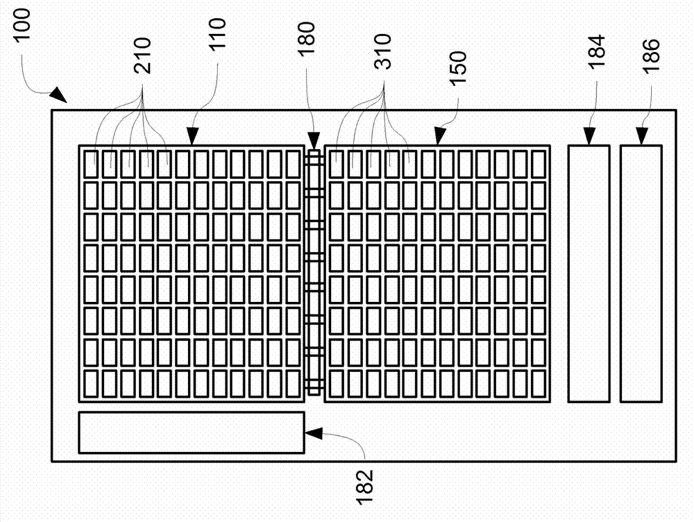
[0040] figure 1 Shown is a demodulation sensor 100 that has been constructed in accordance with the principles of the present invention.

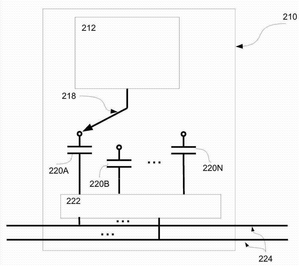
[0041] The illustrated structure extraction element, which is generally integrated into a pixel without being used for light detection, and which is physically separated from the pixel, basically for storage and occasionally processing, is called a memory element or Proxel. Thus, the sensor comprises a pixel array 110 consisting of xXy pixels, and a storage or Proxel array 150 consisting of xXy storage elements or Proxels 310 for further processing, storing information and reading out. Typically x and y are greater than 100, and preferably greater than 200. In some examples x, y are greater than 1000. The two arrays are physically separated from each other, preferably separate arrays that do not physically overlap each other on the chip.

[0042] Multiple functions are preferably handled within the Proxel array 150 . Thus, the sensor 1...


PUM


Abstract

A demodulation image sensor, such as used in time of flight (TOF) cameras, extracts all storage- and post-processing-related steps from the pixels to another array of storage and processing elements (proxels) on the chip. The pixel array has the task of photo-detection, first processing and intermediate storage, while the array of storage and processing elements provides further processing and enhanced storage capabilities for each pixel individually. The architecture can be used to address problems due to the down-scaling of the pixel size. Typically, either the photo-sensitivity or the signal storage capacitance suffers significantly. Both a lower sensitivity and smaller storage capacitances have negative influence on the image quality. The disclosed architecture allows for keeping the storage capacitance unaffected by the pixel down-scaling.

Description

technical field [0001] The present invention relates to a demodulation sensor with a separate pixel and memory array. This application claims benefit under US 35 USC 119(e) of Provisional Patent Application 61 / 292,588 filed January 6, 2010, which is hereby incorporated by reference in its entirety. Background technique [0002] An electronic imaging sensor usually has an m×n photosensitive pixel array with rows X>=1 and columns y>=1. Each pixel of the array is independently addressable by a dedicated readout circuit, corresponding to selection in column order and row order. A unit for signal post-processing can optionally be integrated on the sensor. [0003] Generally the pixel has four basic functions: light detection, signal processing, information storage, and analog or digital conversion. Each of these functions consumes some area on the chip. [0004] A special group of smart pixels, called demodulated pixels, are known for their three-dimensional (3D) imagin...

Claims


Application Information

Patent Timeline
Patent Type & Authority Applications(China)
IPC IPC(8): G01S7/491G01S17/36G01S17/89G01S7/4914G01S17/894
CPCG01S17/89G01S7/4918G01S7/4914G01S17/36G01S7/491G01S17/894
Inventor B·比特根T·欧吉尔
Owner HEPTAGON MICRO OPTICS
Why Eureka
Try Eureka