Improved backdrilling of multilayer printed circuit boards

A technology of printed circuit boards and substrates, which is applied in the direction of printed circuits, printed circuit manufacturing, printed circuit components, etc., and can solve problems such as impact, small via hole to via hole spacing, etc.

Active Publication Date: 2012-12-19
FLEXTRONICS AP LLC
View PDF3 Cites 13 Cited by
  • Summary
  • Abstract
  • Description
  • Claims
  • Application Information

AI Technical Summary

Problems solved by technology

While such backdrilling can eliminate many of the problems associated with via stubs, the larger drill bit creates a larger hole than the original via, which adversely affects: i) Clearance requirements for signal traces on each layer; and ii) minimum via-to-via spacing

Method used


Image

  • Improved backdrilling of multilayer printed circuit boards
  • Improved backdrilling of multilayer printed circuit boards
  • Improved backdrilling of multilayer printed circuit boards

Examples


Embodiment Construction

[0020] While the invention is susceptible to various modifications and alternative forms, specific embodiments thereof have been shown by way of example in the drawings and described in detail herein. It should be understood, however, that there is no intention to limit the invention to the particular forms disclosed, but the intention is to cover all modifications, equivalents, and alternatives falling within the scope and spirit of the invention.

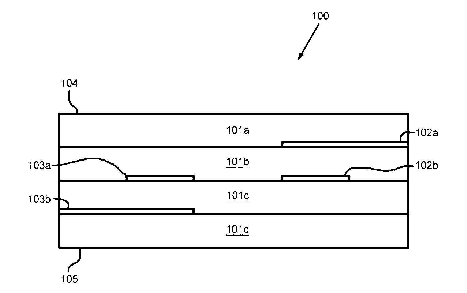
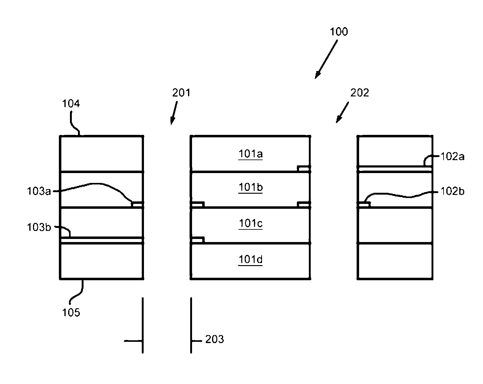
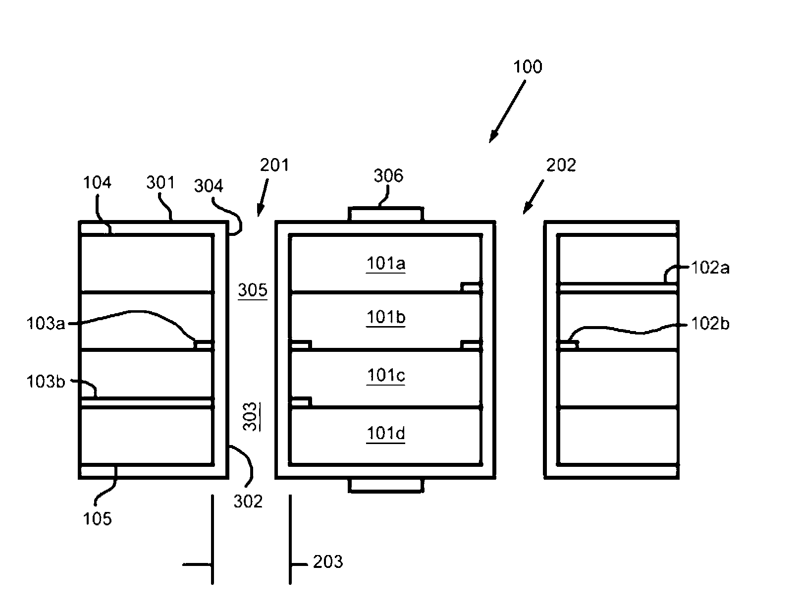
[0021] Embodiments described herein may include PCBs and related manufacturing methods of PCBs in various stages of production. For example, a method of removing via stubs by a combination of backdrilling and chemical etching includes backdrilling the vias to remove the masking layer from the via stubs. After backdrilling is complete, portions of the underlying layer (eg, the conductive layer used to form the conductive path) may remain in the area of ​​the via stub. The remainder of the underlying layer can be removed in a subse...


PUM


Abstract

Methods of backdrilling printed circuit boards (PCBs) to remove via stubs and related apparatuses. The method may include removing a via stub through a combination of backdrilling and chemical etching. The backdrilling may remove a masking layer from the via stub. Portions of an underlying layer may remain in the region of the via stub after the backdrilling is completed. The remaining portions of the underlying layer may be removed in a subsequent etching process thereby removing the via stub from the PCB. As the backdrilling step may be used for the limited purpose of removing the outer layer and portions of the underlying layer remaining in the via can be tolerated, the diameter of the backdrilling need not be as large as traditional backdrilling where all layers within the via must be ensured of being completely removed.

Description

[0001] Cross References to Related Applications [0002] Pursuant to Title 35, United States Code, Section 119, this application claims priority to U.S. Provisional Application No. 61 / 319,371, filed March 31, 2010, entitled "Backdrilling of Multilayer Printed Circuit Boards," the entirety of which The contents are incorporated herein by reference. Background technique [0003] Typically, a printed circuit board (PCB) contains a plurality of vias, each via electrically connecting a conductive trace on one layer of the PCB to one or more conductive traces on one or more other layers of the PCB. Some vias may be interconnected such that a portion of the via is not located along a conductive portion of the PCB. For example, in the case of a via interconnecting two inner layers of a PCB, the portion of the via extending from the outermost one of the inner layers to the surface of the PCB is called a via stub. Via stubs do not serve a useful function in the circuitry of the PCB an...

Claims


Application Information

Patent Timeline
IPC IPC(8): H05K3/40B23B41/00
CPCH05K2203/0207H05K3/429H05K1/0251H05K3/0047Y10T29/49156Y10T29/49165Y10T29/49167
Inventor 刘卓平
Owner FLEXTRONICS AP LLC
Why Eureka
Try Eureka