Preparation system and method of gallium nitride-based materials and devices

A gallium nitride-based, preparation system technology, applied in the field of microelectronics, can solve problems such as the difficulty of growing gallium nitride materials, lattice mismatch thermal mismatch, cracking of gallium nitride materials, etc., to reduce the current collapse effect, The effect of avoiding surface oxidation problems and improving quality

Active Publication Date: 2016-08-17
ENKRIS SEMICON
View PDF8 Cites 0 Cited by
  • Summary
  • Abstract
  • Description
  • Claims
  • Application Information

AI Technical Summary

Problems solved by technology

[0004] It is quite difficult to grow GaN material on silicon. There is a huge lattice mismatch and thermal mismatch between silicon and GaN. If stress engineering is not used, GaN material on silicon will crack and severe warping of the silicon substrate

Method used


Image

  • Preparation system and method of gallium nitride-based materials and devices
  • Preparation system and method of gallium nitride-based materials and devices
  • Preparation system and method of gallium nitride-based materials and devices

Examples


Embodiment Construction

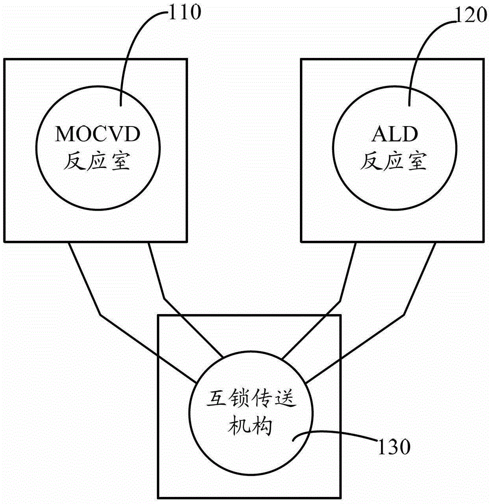
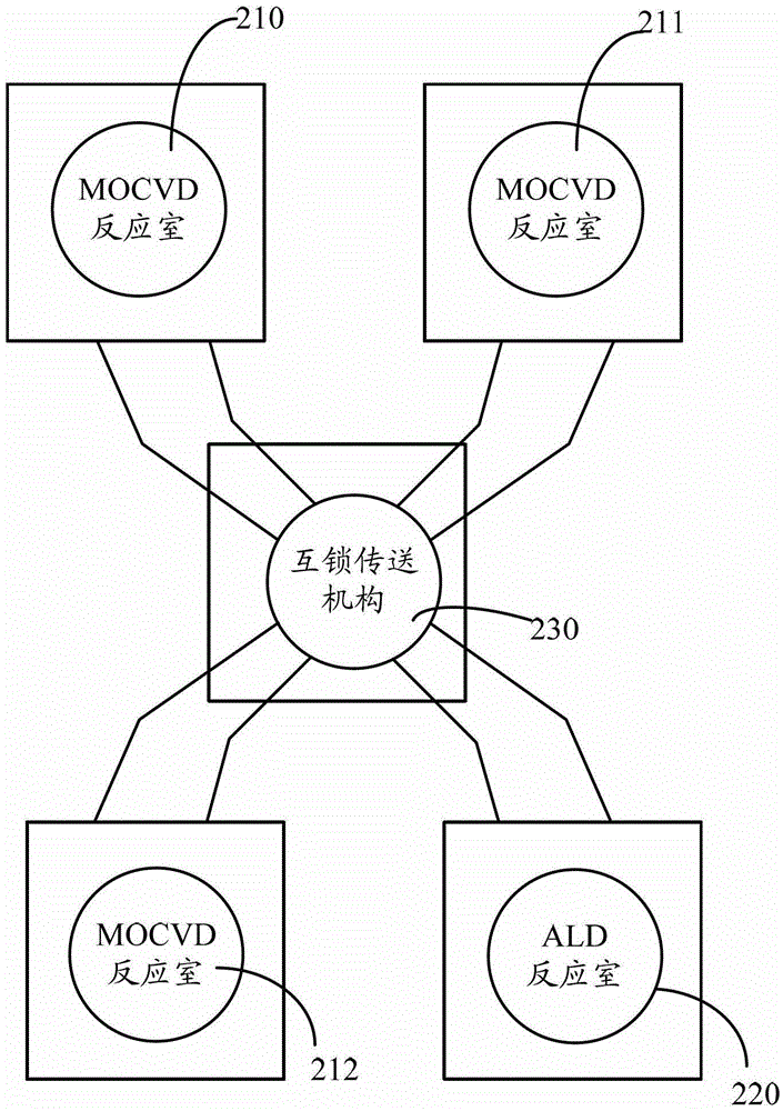
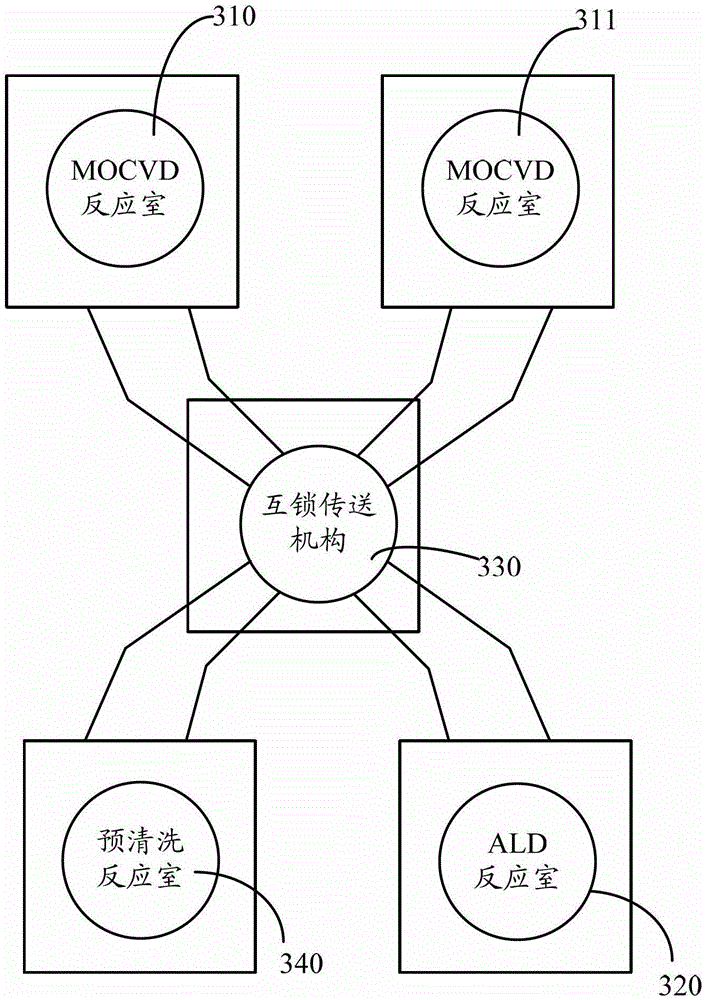
[0047] A system for preparing gallium nitride-based materials and devices of the present invention is an integrated system and includes:

[0048] One or more MOCVD reaction chambers;

[0049] One or more ALD reaction chambers;

[0050] And the interlocking transmission mechanism connected with the MOCVD reaction chamber and the ALD reaction chamber

[0051] Correspondingly, the preparation method of a gallium nitride-based material and device of the present invention includes:

[0052] Provide one or more MOCVD reaction chambers and one or more ALD reaction chambers;

[0053] Using the interlocking transfer mechanism, the gallium nitride-based materials to be grown are sequentially entered into different reaction chambers to grow corresponding epitaxial layers, or the devices to be processed are sequentially entered into different reaction chambers for corresponding processes. The reaction chamber works under the corresponding conditions, with corresponding gas or liquid or plasma input...


PUM


Abstract

The present invention discloses a preparation system and a preparation method for a gallium nitride base material and a device thereof. The system is an integrated system, which comprises one or a plurality of MOCVD reaction chambers, one or a plurality of ALD reaction chambers, and an interlock transport mechanism connected with the MOCVD reaction chamber and the ALD reaction chamber. The MOCVD reaction chamber can be a standard structure, and is provided for nitride growth. The ALD reaction chamber can be provided for concurrently growing a nitride medium layer and an oxide medium layer, wherein the maximum growth temperature can reach more than 500 DEG C, and a high quality oxide film or a high quality nitride film can grow. In addition, a pre-cleaning chamber can be optionally arranged, and is provided for cleaning the surface of a substrate or a nitride. With the integrated system, cleaning, epitaxial layer growth and medium layer growth can be concurrently completed so as to avoid contamination in air. With the present invention, qualities of the crystal and the medium layer can be substantially improved, device performances can be improved, and novel device structures can be prepared.

Description

Technical field [0001] The invention relates to the technical field of microelectronics, and in particular to a preparation system and preparation method of gallium nitride-based materials and devices. Background technique [0002] Gallium nitride is considered to be the most important semiconductor material after silicon. Gallium nitride is a wide bandgap semiconductor material. Its spectrum covers the entire visible light region. It can be made into blue and white light emitting diodes for display, TV backlighting and general lighting; it can be made into green / blue light emitting diodes. Together with AlGaInP-based red light-emitting diodes, it is used for full-color display; it can also be made into ultraviolet lasers for data storage. In addition to excellent optical properties, the electrical properties of gallium nitride are also excellent: high electron mobility (~2000cm 2 / Vs), high electron velocity (2.5E7cm / s), high critical electric field (3.5MV / cm), etc. Therefore,...

Claims


Application Information

Patent Timeline
Patent Type & Authority Patents(China)
IPC IPC(8): C30B25/02C30B29/38H01L21/20H01L33/00
Inventor 程凯
Owner ENKRIS SEMICON
Why Eureka
Try Eureka