
Patsnap Eureka
For R&D, Patsnap Eureka makes reading and utilizing patents & technical documents easy.
Patsnap Eureka AIR
Designed for self-driven R&D workflows. Generate viable solutions, solve complex R&D challenges, empower your innovation with AI.

Patsnap Eureka Materials
Designed for material experts only. Revolutionize your material R&D, from search, analyze, to developing new materials.

TechResearch
Generate reliable direction feasibility study reports for your R&D in just a few steps.

TechSeek
Discover and master advanced knowledge NOW. Basics, ideas, possibilities, all at once.

TechMind
As an expert in R&D Theories, TechMind can generates customized viable solutions instantly.

TechRisk
Analyze your overall solution with one click, know your potential R&D risks in advance.

TechMonitor
Get weekly tech updates, stay abreast of the latest tech innovations and key insights.
Method for improving clearness of alignment marks
An alignment mark and clarity technology, applied in the field of improving alignment mark clarity, can solve problems such as alignment failures in lithography steps, and achieve the effect of eliminating alignment failures and improving accuracy
- Summary
- Abstract
- Description
- Claims
- Application Information
AI Technical Summary
Problems solved by technology
Method used
Image

Examples
Embodiment Construction
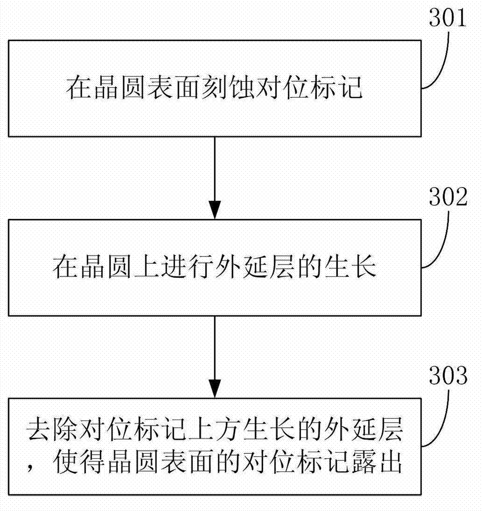
[0027] The technical solutions of the present invention will be further described below in conjunction with the accompanying drawings and through specific implementation methods. It should be understood that the specific embodiments described here are only used to explain the present invention, but not to limit the present invention. It should also be noted that, for ease of description, only steps related to the present invention are shown in the drawings but not all processes.
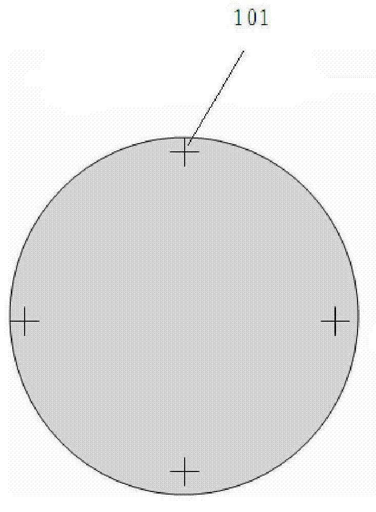
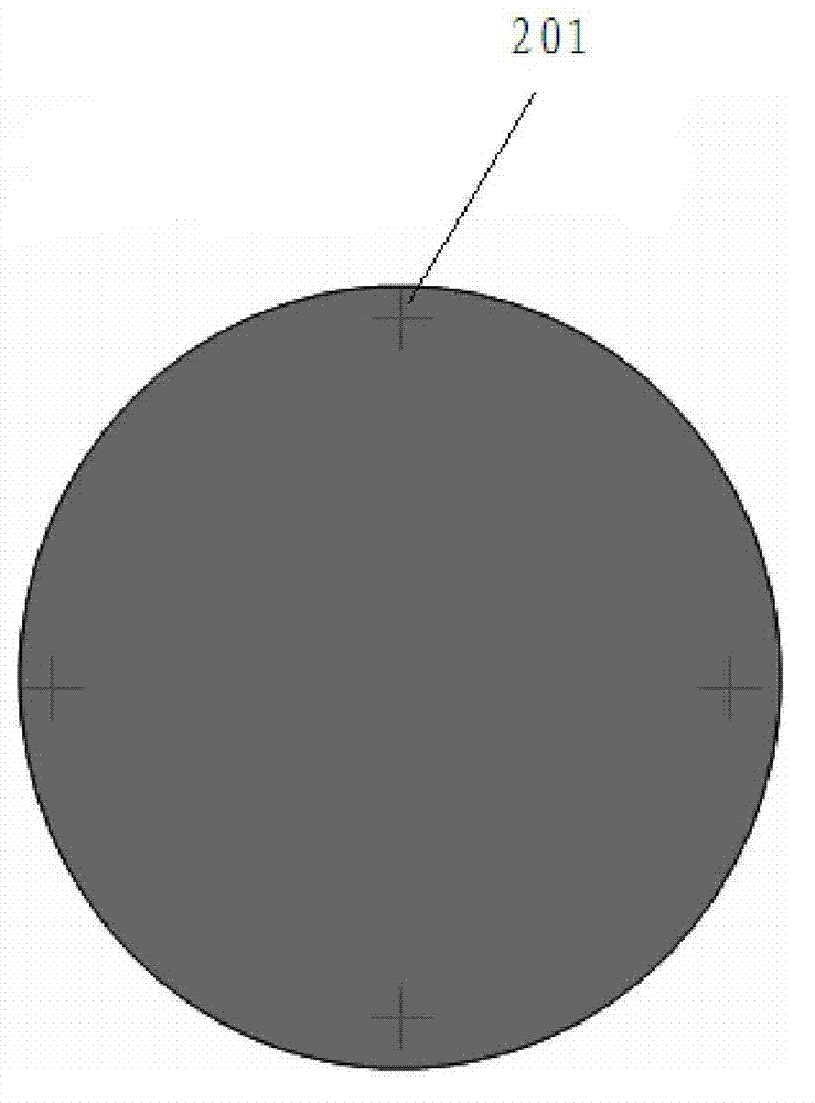
[0028] image 3 It is a flow chart of the method for improving the definition of alignment marks provided by the first embodiment of the present invention. Such as image 3 As shown, the method includes:
[0029] Step 301 , etching an alignment mark on the surface of the wafer.
[0030] In one embodiment of the present invention, it can be as figure 1 As shown, a laser is used to etch the alignment mark, and a cross-shaped alignment mark is punched at predetermined positions on the upper, lower,...
PUM
 Abstract
Description
Claims
Application Information
 - R&D Engineer
- R&D Manager
- IP Professional
- Industry Leading Data Capabilities
- Powerful AI technology
- Patent DNA Extraction
Browse by: Latest US Patents, China's latest patents, Technical Efficacy Thesaurus, Application Domain, Technology Topic, Popular Technical Reports.
© 2024 PatSnap. All rights reserved.Legal|Privacy policy|Modern Slavery Act Transparency Statement|Sitemap|About US| Contact US: help@patsnap.com