Device for monitoring stability of optical path of photoetching equipment

A lithography equipment and a technology for monitoring light, which are applied in microlithography exposure equipment, photolithography exposure devices, and testing optical properties, etc., can solve the problems of inability to monitor in real time, cumbersome optical path procedures and equipment, and increased production costs Risk and other issues, to avoid downtime monitoring conditions, reduce production costs, and improve efficiency

Active Publication Date: 2013-01-09
SHANGHAI HUALI MICROELECTRONICS CORP
View PDF5 Cites 2 Cited by
  • Summary
  • Abstract
  • Description
  • Claims
  • Application Information

AI Technical Summary

Problems solved by technology

[0007] When the light deviation occurs, the monitoring and testing of the optical path requires very cumbersome procedures and equipment, and it often takes more than 6 hours of downtime to measure a data point, which is unbearable in mass production, and because of the light The detection is only discovered after the offset, and real-time monitoring is impossible, which greatly increases the risk of production costs

Method used


Image

  • Device for monitoring stability of optical path of photoetching equipment
  • Device for monitoring stability of optical path of photoetching equipment
  • Device for monitoring stability of optical path of photoetching equipment

Examples


Embodiment Construction

[0027] The specific embodiment of the present invention will be further described below in conjunction with accompanying drawing:

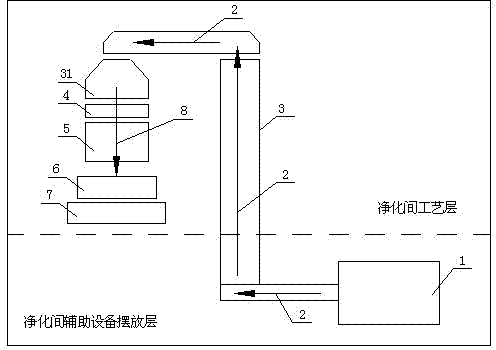
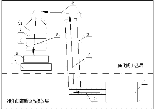
[0028] Figure 4 It is a structural schematic diagram of the device for monitoring the stability of the optical path of the lithography equipment in the present invention;

[0029] Such as Figure 4 As shown, the present invention is a device for monitoring the stability of the optical path of lithography equipment. A level 9 is provided on each optical path lens 3 passing by the illumination optical path 2, and a level 9 is also arranged on the optical path lens 31 passed by the projection optical path 3. At the same time, a level 9 is also set on the shock absorber 7 of the lithography machine; wherein, the level 9 is a mechanical level or an electronic level, and each level 9 is connected to the lithography information management system (not shown in the figure). The information management system can check the real-time data of each level 9 i...


PUM


Abstract

The invention relates to the field of semiconductor manufacturing, and in particular relates to a device for monitoring stability of an optical path of photoetching equipment. According to the device for monitoring the stability of the optical path of the photoetching equipment, leveling instruments are arranged on an illumination optical path device and a projection optical path device of the photoetching equipment, so that the offset of deviation of the optical path in monitoring equipment is realized to adjust a photoetching machine, and therefore, a stop monitoring condition caused by the overlarge offset of deviation of the optical path is effectively avoided, the monitoring efficiency of the offset of deviation of the optical path is effectively improved, and the production cost is reduced.

Description

technical field [0001] The invention relates to the field of semiconductor manufacturing, in particular to a device for monitoring the stability of an optical path of a lithography equipment. Background technique [0002] At present, with the continuous improvement of integrated circuit manufacturing technology and the continuous shrinking of line width, the area of ​​semiconductor devices is becoming smaller and smaller. The layout of semiconductors has evolved from ordinary single-function separation devices to integrated high-density multi-functional integration Circuit; from the initial integrated circuit (IC) to large-scale integrated circuit (LSI), very large-scale integrated circuit (VLSI), until today's ultra-large-scale integrated circuit (ULSI), the area of ​​the device is further reduced, and the function is more comprehensive and powerful . Considering the complexity of process research and development, long-term and high cost and other unfavorable factors, how ...

Claims


Application Information

Patent Timeline
Patent Type & Authority Applications(China)
IPC IPC(8): G03F7/20G01M11/02
Inventor 朱骏张旭昇
Owner SHANGHAI HUALI MICROELECTRONICS CORP
Why Eureka
Try Eureka