Optoelectronic component and method for producing an optoelectronic component

A technology of optoelectronic devices and luminescent materials, applied in the direction of electric solid devices, optical components, electrical components, etc., can solve the problems of particle density gradient consumption, difficult to reproduce, expensive, etc., and achieve the effect of uniform optical density and high optical efficiency

Active Publication Date: 2013-01-09
OSRAM OPTO SEMICONDUCTORS GMBH & CO OHG
View PDF7 Cites 0 Cited by
  • Summary
  • Abstract
  • Description
  • Claims
  • Application Information

AI Technical Summary

Problems solved by technology

However, the adjustment of the gradient of the particle density is extremely complex, difficult to reproduce and expensive in production

Method used


Image

  • Optoelectronic component and method for producing an optoelectronic component
  • Optoelectronic component and method for producing an optoelectronic component
  • Optoelectronic component and method for producing an optoelectronic component

Examples


Embodiment Construction

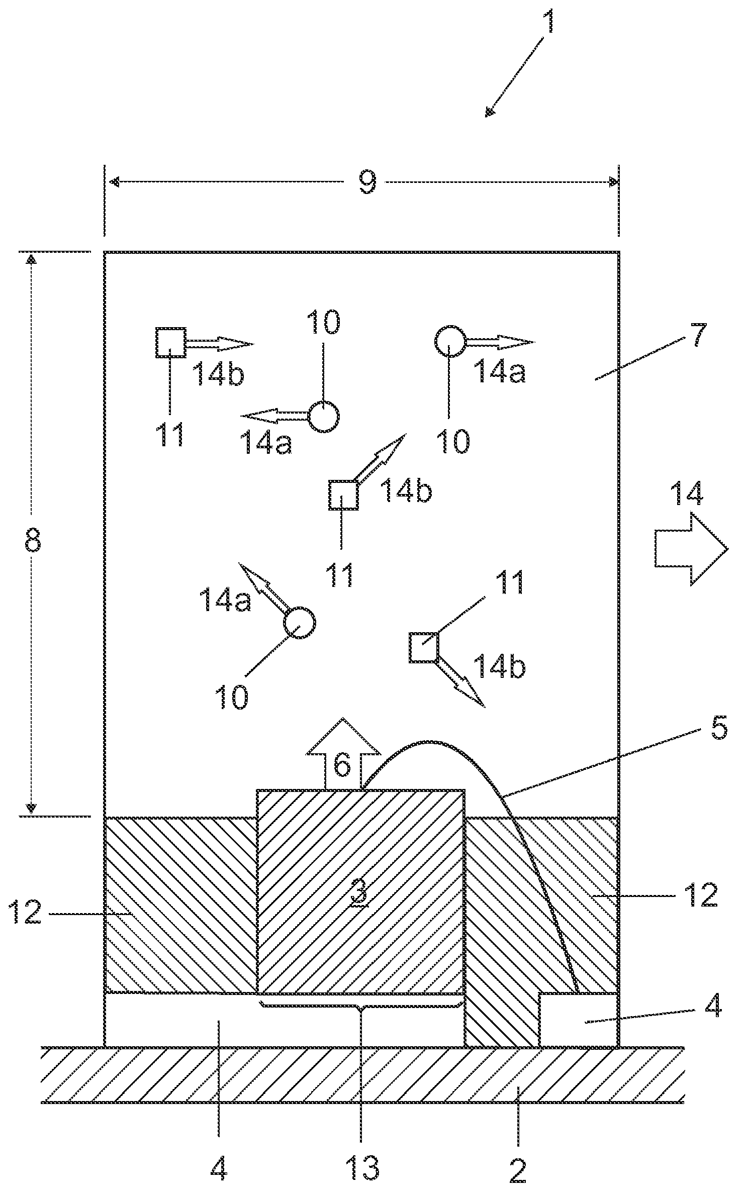
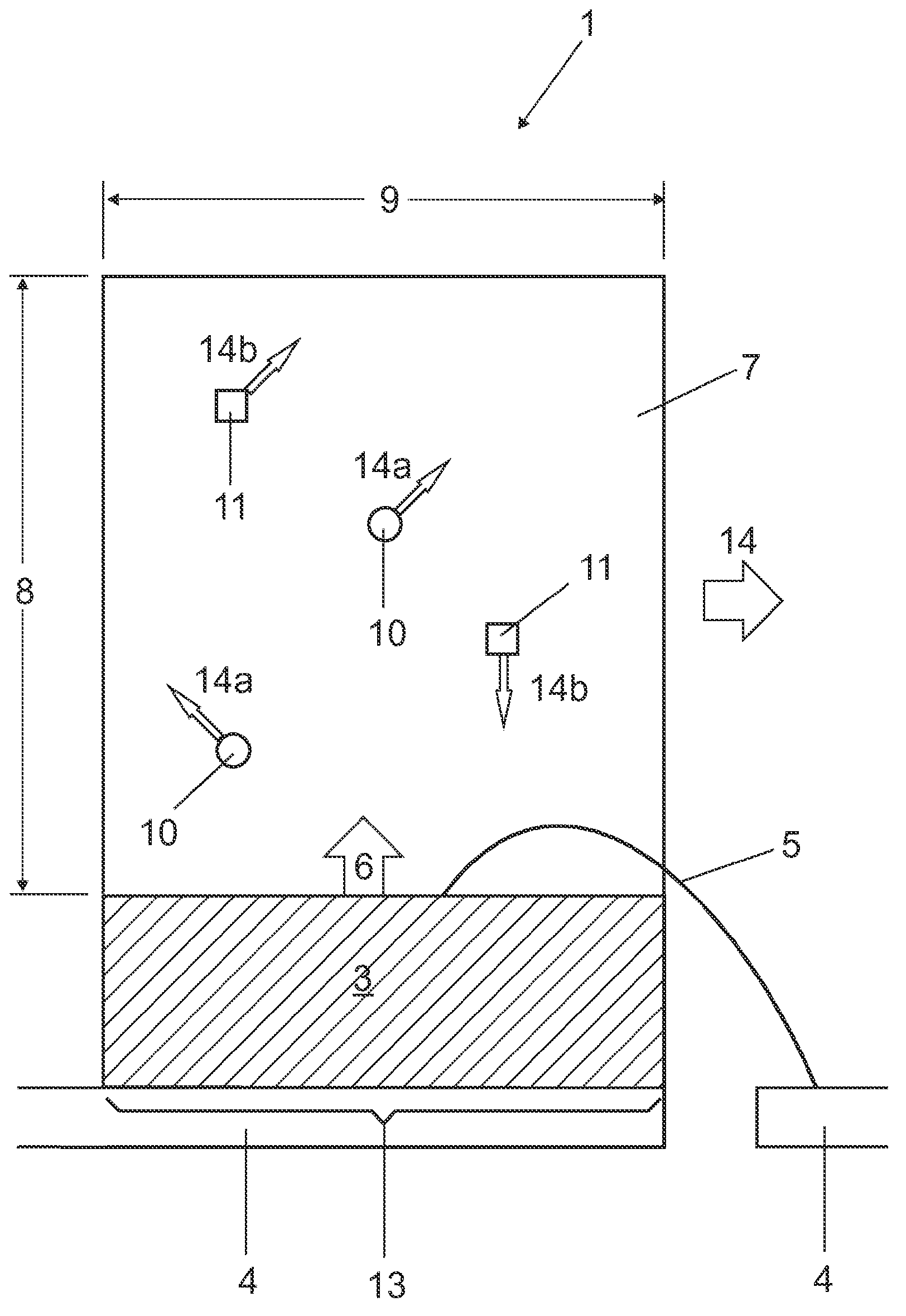
[0055] Identical, similar or identically acting elements are provided with the same reference symbols in the figures. The drawings and the size ratios of the elements shown in the drawings to each other cannot be shown to be to scale. On the contrary, individual elements can be shown exaggerated for better description and better understanding.

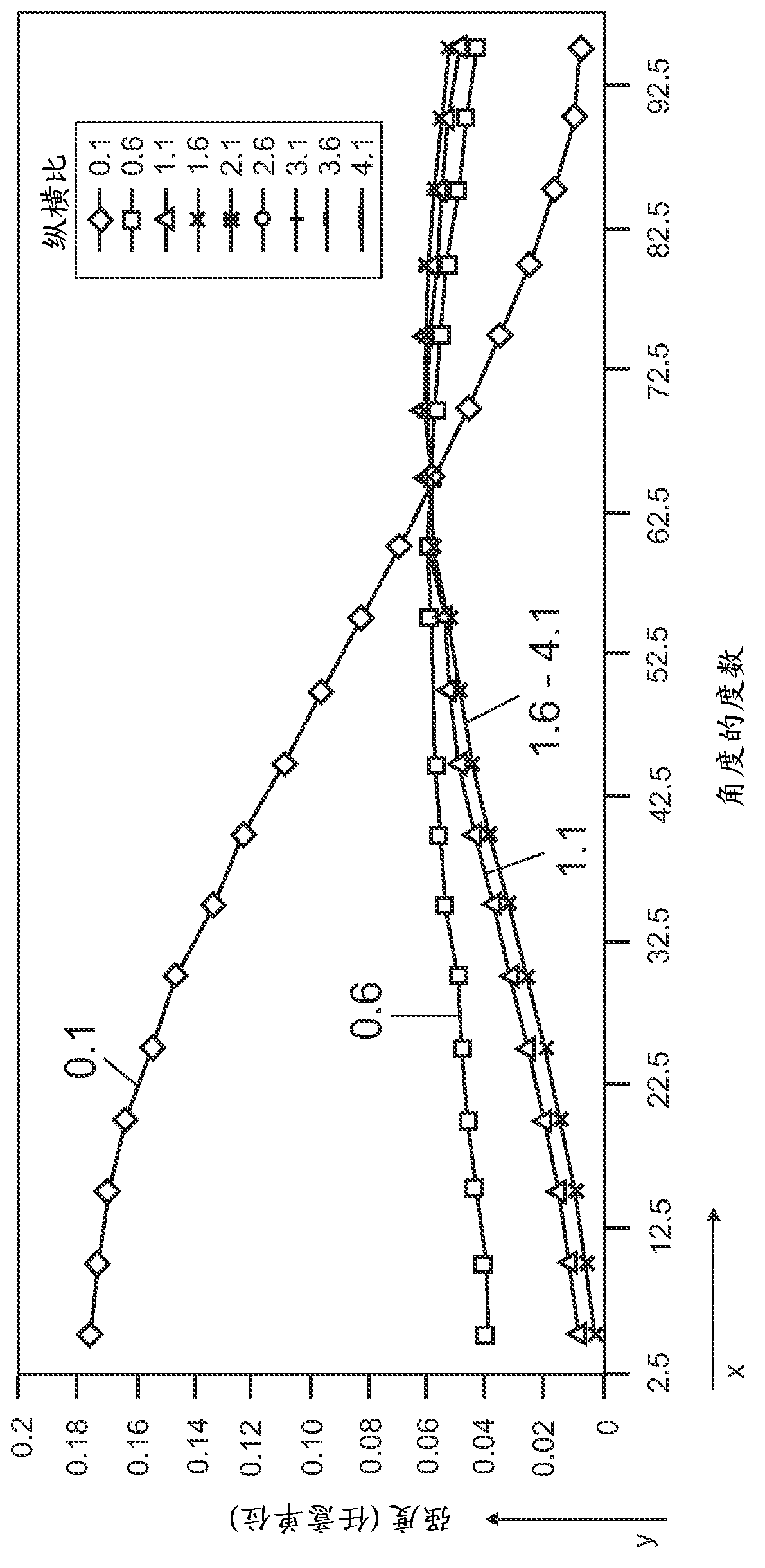
[0056] figure 1 An optoelectronic component 1 is shown. A semiconductor chip 3 is applied on the carrier 2 . Electrical contacting is effected via contacts 4 and bonding wires 5 . The semiconductor chip 3 emits primary radiation 6 . The semiconductor chip 3 is at least partially surrounded by an at least partially transparent medium 7 having a height 8 above the carrier 2 and a width 9 (aspect ratio) along the carrier 2 . Particles 10 , 11 interacting with primary radiation 6 are introduced into medium 7 . The medium 7 has an aspect ratio greater than one. The particles 10 , 11 are evenly distributed in the medium 7 . The parti...


PUM


Abstract

An optoelectronic component (1) comprises a carrier (2) and at least one semiconductor chip (3). The semiconductor chip (3) is arranged on the carrier (2) and equipped to emit a primary radiation (6). The semiconductor chip (3) is enclosed at least partially by an at least partially transparent medium (7) having a height (8) above the carrier (2) and a width (9) along the carrier (2). Particles (10, 11) that interact with the primary radiation (6) are introduced into the medium (7). The medium (7) has a ratio of height (8) to width (9) of more than 1.

Description

technical field [0001] The invention relates to an optoelectronic component having a semiconductor chip for emitting electromagnetic radiation, and to a lighting arrangement having at least one such optoelectronic component. Furthermore, a method for producing an optoelectronic component is proposed. Background technique [0002] Optoelectronic components and light-emitting devices having such optoelectronic components are known from the prior art. Document WO 2009 / 135620 A1 thus discloses a lighting device having a lighting means emitting electromagnetic radiation. A refinement of the lighting means can be an optoelectronic component. The electromagnetic radiation is partly deflected and partly changed in relation to its wavelength by the interaction with the particles. The deflection of electromagnetic radiation can be achieved by gradients in particle density. However, the adjustment of the particle density gradient is extremely complex, difficult to reproduce and exp...

Claims


Application Information

Patent Timeline
Patent Type & Authority Applications(China)
IPC IPC(8): H01L33/48H01L33/50H01L33/56H01L33/54G02B6/00H01L33/60
CPCH01L2933/0091G02B6/0023H01L33/501H01L33/56H01L33/60G02B6/0073H01L2224/48091H01L2224/8592H01L33/505H01L33/502H01L2924/00014H01L33/62
Inventor 斯特凡·伊莱克亚历山大·林科夫马蒂亚斯·扎巴蒂尔
Owner OSRAM OPTO SEMICONDUCTORS GMBH & CO OHG
Why Eureka
Try Eureka