Manufacturing method of high-voltage alternating semiconductor LED (light-emitting diode) chips

A light-emitting diode, high-voltage AC technology, applied in semiconductor devices, electrical solid-state devices, electrical components, etc., can solve the problems of the whole chip not working properly, unfavorable for integrated chips, and occupying a large area, so as to reduce the occupied area and avoid Connection method, the effect of improving the efficiency of use

Inactive Publication Date: 2013-01-23
施科特光电材料(昆山)有限公司
View PDF3 Cites 5 Cited by
  • Summary
  • Abstract
  • Description
  • Claims
  • Application Information

AI Technical Summary

Problems solved by technology

However, the current high-voltage AC LED chip is just a simple series-parallel connection of low-power chips, and the structure of its components is relatively complicated. If a node is abnormal, the entire chip cannot work normally.
In addition, its relatively large footprint is not conducive to integrating more chips

Method used


Image

  • Manufacturing method of high-voltage alternating semiconductor LED (light-emitting diode) chips
  • Manufacturing method of high-voltage alternating semiconductor LED (light-emitting diode) chips
  • Manufacturing method of high-voltage alternating semiconductor LED (light-emitting diode) chips

Examples


Embodiment Construction

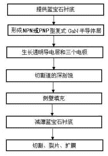
[0044] The specific implementation of the manufacturing method of the high-voltage AC semiconductor light-emitting diode chip of the present invention will be explained below in conjunction with the accompanying drawings. However, implementation of the present invention is not limited to the following embodiments.

[0045] Explanation: the accompanying drawings of the present invention are only schematic diagrams, and the representations in the drawings are only schematic in nature. In the drawings, in order to clearly reflect the principles and structures of the present invention, the thicknesses of layers and regions have been appropriately adjusted, and they are not strictly used as schematic diagrams. Reflecting the proportional relationship of aggregate size, therefore, the schematic diagram of the present invention cannot be used to limit the scope of the present invention.

[0046] A method for manufacturing a high-voltage AC semiconductor light-emitting diode chip, com...


PUM


Abstract

The invention relates to the design and manufacturing of LED (light-emitting diode) chips, and relates to a manufacturing method of a high-voltage alternating semiconductor LED chip. The manufacturing method comprises the following steps: (1) providing a sapphire substrate; (2) forming a compound GaN semiconductor layer; (3) growing a transparent conductive layer and three electrodes; (4) carrying out deep etching on a cutting channel; (5) filling a side wall; (6) thinning the sapphire substrate; and (7) cutting, splitting and expanding a membrane. The preparation method provided by the invention is conductive to lowering the production cost and improving the using efficiency, and is suitable for industrial large-scale production; and the high-voltage alternating semiconductor LED chip provided by the method provided by the invention has the advantages of the high-voltage alternating chip, also can prevent a complex connecting mode, can be used for reducing the occupied area of the chip, achieving LED chip integration and facilitating the realization of the serial and parallel connection of chips, and has the advantages of a functional component.

Description

technical field [0001] The invention relates to the technical field of semiconductor materials, and relates to the design and manufacture of LED chips, in particular to a GaN-based compound structure (NPN, PNP) light-emitting diode chip and a manufacturing method thereof that can be directly connected to alternating current. Background technique [0002] Light-emitting diode (LED) is a new generation of solid-state light source. It has many advantages such as small size, low power consumption, long service life, high luminous efficiency, low heat, environmental protection and energy saving, and durability. It is widely used in image display, signal indication and lighting. lamp field. In recent years, driven by new technologies, the research and manufacture of gallium nitride (GaN)-based light-emitting diodes has developed rapidly. GaN-based LED is currently recognized as a major achievement in optoelectronic science and technology, and is a key light source for the develop...

Claims


Application Information

Patent Timeline
Patent Type & Authority Applications(China)
IPC IPC(8): H01L33/00H01L33/36H01L33/20H01L25/075
Inventor 杨旅云陈晓鹏张宇欣张国龙吴东平常志伟薛进营王明辉夏成
Owner 施科特光电材料(昆山)有限公司
Why Eureka
Try Eureka