Gate drive circuit for output linear current of metal oxide semiconductor field effect transistor

A technology of oxide semiconductors and field effect transistors, which is applied in the field of metal oxide semiconductor field effect transistor voltage-to-current conversion drive circuits, can solve problems affecting output accuracy, cost increase, and process differences affecting circuit linearity, etc., to achieve circuit The effect of simple components and reduced manufacturing costs

Active Publication Date: 2017-04-19
UP SHINE LIGHTING CO
View PDF4 Cites 0 Cited by
  • Summary
  • Abstract
  • Description
  • Claims
  • Application Information

AI Technical Summary

Problems solved by technology

It combines the amplifier and the current mirror circuit to become an active current mirror differential pair, and the control voltage V in Input from the positive terminal of the amplifier, controlled by negative feedback, the virtual short circuit characteristic of the amplifier makes the resistance R s The upper terminal voltage is V -n , through resistor R s The amount of current is I out =V in / R s , current I out The output is converted by the current mirror; if the voltage source is 5V, when I out Level must be 10 -9 A, the resistor R s It takes 10 6 Ω level or above, polysilicon is used as the resistor in the chip, 10 6 In addition to requiring a large area to increase the cost of the Ω-level resistance value, the resistance value of polysilicon as a resistor can vary by up to ±25% due to process differences, which will affect the output accuracy.
There are also many voltage-current conversion methods that do not use resistors. Most of them use complex circuits to offset the nonlinear term in the MOSFET current formula, so that the output current calculation formula becomes a linear linear formula. In addition to the increase in cost, process differences will also affect the linearity of the circuit output. These are the areas where the voltage-current conversion circuit needs to be improved.

Method used


Image

  • Gate drive circuit for output linear current of metal oxide semiconductor field effect transistor
  • Gate drive circuit for output linear current of metal oxide semiconductor field effect transistor
  • Gate drive circuit for output linear current of metal oxide semiconductor field effect transistor

Examples


Embodiment Construction

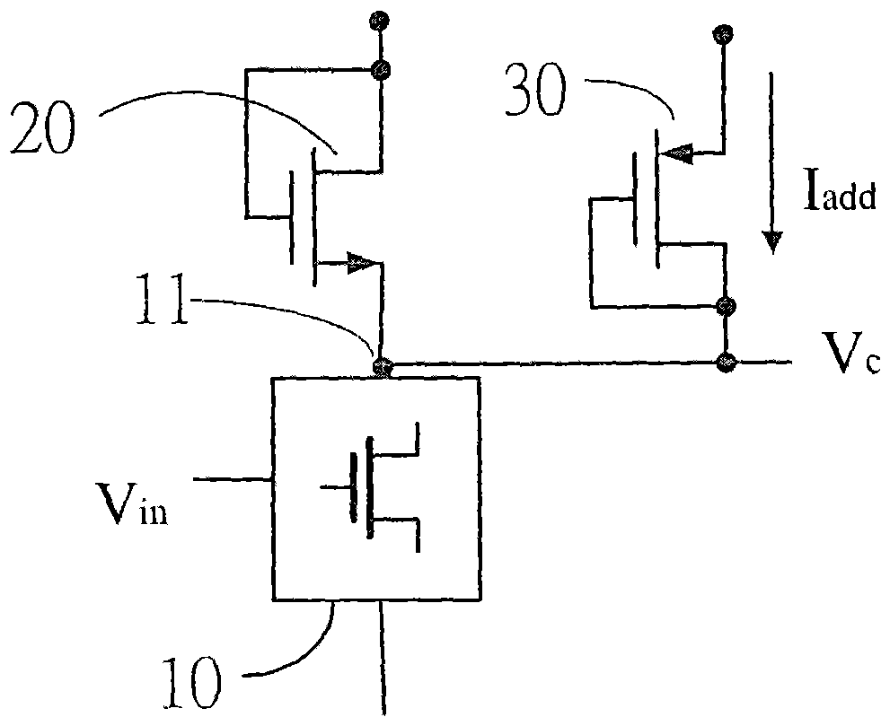
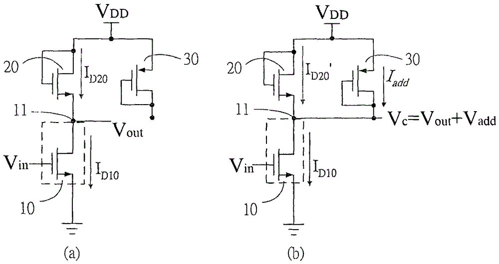
[0037] The detailed technical contents of the present invention will be clearly presented by presenting the embodiments matched with the illustrations. In the description, the size of the metal oxide semiconductor field effect transistor is defined as the (width / length) ratio of the element channel, expressed in (W / L) XX Indicates that the numbers subscripted by each symbol " XX ” is the component number in the illustration.

[0038] see figure 2 , is the basic structure embodiment of the gate drive circuit of the present invention that makes the metal oxide semiconductor field effect transistor output linear current, a gate terminal is connected to the drain terminal N-type metal oxide semiconductor field effect transistor 20, a gate terminal is connected to the drain terminal The P-type metal oxide semiconductor field effect transistor 30 connected to the extreme, a voltage input circuit 10; the voltage input circuit 10 includes at least one metal oxide semiconductor fiel...


PUM


Abstract

A grid drive circuit for a metallic oxide semiconductor field effect transistor to output a linear current is provided. The grid drive circuit comprises a P-type metallic oxide semiconductor field effect transistor of diode connection configuration, an N-type metallic oxide semiconductor field effect transistor of diode connection configuration, and a voltage input circuit at least including a metallic oxide semiconductor field effect transistor. If an output voltage of the grid drive circuit is connected to a grid electrode of a metallic oxide semiconductor field effect transistor, the metallic oxide semiconductor field effect transistor outputs a current having a linear relationship with an input voltage. According to the invention, the circuit and the elements are simple, reducing production cost.

Description

technical field [0001] The invention relates to a gate drive circuit for making a metal oxide semiconductor field effect transistor output a linear current, in particular to a voltage-to-current conversion drive circuit for a metal oxide semiconductor field effect transistor with a simple structure. Background technique [0002] In digital circuits, the control terminal generally receives a voltage signal input, and some controls need to convert the input linear voltage into a linear current output, such as a voltage-controlled oscillator (VCO) in a phase-locked loop (PLL). It is converted into current in proportion; and when transmitting digital voltage signals over long distances, the resistance of the transmission line will attenuate the voltage signal, so the voltage signal must be converted into current before being transmitted in the form of current to reduce the influence of transmission line impedance on the signal. [0003] A known voltage-to-current converter is sh...

Claims


Application Information

Patent Timeline
Patent Type & Authority Patents(China)
IPC IPC(8): H03K17/687
Inventor 陈于强苏宗才谢祖华
Owner UP SHINE LIGHTING CO
Why Eureka
Try Eureka