Image sensor with doped transfer gate

An image sensor and transfer gate technology, applied in the field of image sensors, can solve problems affecting the electrical operation of the transfer gate, etc.

Active Publication Date: 2013-01-30
OMNIVISION TECH INC
View PDF4 Cites 1 Cited by
  • Summary
  • Abstract
  • Description
  • Claims
  • Application Information

AI Technical Summary

Problems solved by technology

Removing the doped region 122 will change the work function of the transfer...

Method used


Image

  • Image sensor with doped transfer gate
  • Image sensor with doped transfer gate
  • Image sensor with doped transfer gate

Examples


Embodiment Construction

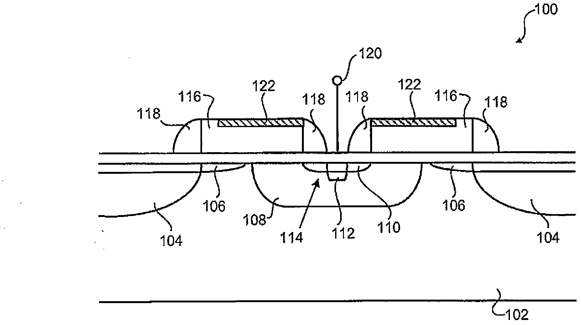
[0024] In the specification and claims, the following terms take the meanings explicitly associated herein, unless the context clearly dictates otherwise. The meanings of "a" and "the" include plural references, and the meaning of "in" includes "in" and "on". The term "connected" means a direct electrical connection between connected items, or an indirect connection through one or more passive or active intermediary devices. The term "circuitry" means a single component or multiple components (active or passive) connected together to provide a desired function. The term "signal" means at least one charge packet, current, voltage or data signal.

[0025] Furthermore, directional terms such as "on", "above", "top", "bottom" are used with reference to the orientation of the figures described. Because components of embodiments of the present invention may be positioned in many different orientations, directional terms are used for purposes of illustration only and are not limiti...


PUM


Abstract

An image sensor includes an array of pixels, with at least one pixel including a photodetector formed in a substrate layer and a transfer gate disposed adjacent to the photodetector. The substrate layer further includes multiple charge-to-voltage conversion regions. A single photodetector can transfer collected charge to a single charge-to-voltage conversion region, or alternatively multiple photodetectors can transfer collected charge to a common charge-to- voltage conversion region shared by the photodetectors. An implant region formed when dopants are implanted into the substrate layer to form source/drain implant regions is disposed in only a portion of each transfer gate while each charge-to-voltage conversion region is substantially devoid of the implant region.

Description

technical field [0001] The present disclosure relates generally to image sensors, and more particularly, to image sensors having implanted regions formed in only a portion of the transfer gate during implantation of source / drain regions. Background technique [0002] FIG. 1 is a cross-sectional view of a part of an image sensor according to the related art. Image sensor 100 includes substrate 102 having photodetector 104, threshold implant 106, well 108, lightly doped drain (LDD) 110, and heavy source / drain implant region 112 formed therein. The combination of well 108 , LDD 110 and source / drain implant region 112 serves as charge-to-voltage conversion region 114 . Well 108 also operates as a breakdown resistant region between LDD 100 or source / drain implant region 112 to photodetector 104 . [0003] Threshold implant 106 and well 108 are formed before transfer gate 116 is created, while photodetector 104 and LDD 110 are formed after transfer gate 116 is formed. Because p...

Claims


Application Information

Patent Timeline
IPC IPC(8): H01L27/146
CPCH01L27/14603H01L27/14609H01L27/14689H01L27/14612H01L27/14806
Inventor 洪·阔克·多恩埃里克·戈登·史蒂文斯
Owner OMNIVISION TECH INC
Why Eureka
Try Eureka