Detection device and method for position and inclination angle of chip

A chip and patch technology, which is applied in the field of devices for performing detection of position and inclination angle, can solve the problems of decreased accuracy, increased cost, insufficient detection accuracy, etc., and achieves the effects of compact device structure, convenient practical operation, and wide application prospects.

Active Publication Date: 2013-02-27
GUANGDONG JUHUA PRINTING DISPLAY TECH CO LTD
View PDF3 Cites 18 Cited by
  • Summary
  • Abstract
  • Description
  • Claims
  • Application Information

AI Technical Summary

Problems solved by technology

[0003] In the prior art, the method for detecting the position of the chip in the chip placement process is generally to use a CCD to directly take pictures of the chip, and obtain information about the position of the chip after processing the captured image. Complicated and other disadvantages; and the operation of obtaining chip position information (upper view acquisition) and substrate position acquisition (bottom view acquisition)

Method used


Image

  • Detection device and method for position and inclination angle of chip

Examples


Embodiment Construction

[0025] In order to make the object, technical solution and advantages of the present invention clearer, the present invention will be further described in detail below in conjunction with the accompanying drawings and embodiments. It should be understood that the specific embodiments described here are only used to explain the present invention, not to limit the present invention.

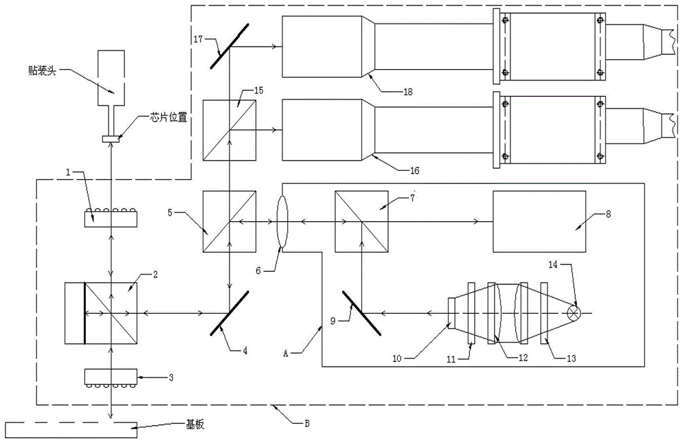
[0026] figure 1 It is a schematic diagram of the overall structure of the chip position and inclination detection device according to the present invention. Such as figure 1 As shown in , according to the present invention, the device for detecting the position and inclination of the chip in the chip placement process mainly includes a light source component, an optical path transmission component, a camera component, and an autocollimator. The light source assembly is composed of a first light source 1 and a second light source 3 such as a ring light source, which are arranged corresponding to t...


PUM


Abstract

The invention discloses a detection device for position and inclination angle of a chip, which comprises a light source component, a light transmission component, a photographing component and an autocollimator, wherein the light source component is constituted by a first light source and a second light source respectively corresponding to the chip and a substrate; the light transmission component is constituted by a first transflective prism, a second transflective prism and a third transflective prism, as well as a first reflector and a second reflector, so that detecting the position of the chip and the substrate is realized in an identical light path system; the photographing component is constituted by a first photographing unit and a second photographing unit which have different visual fields; the first photographing unit is used for collecting images with large visual fields of the chip or the substrate, realizing primary location according to MARK points; the second photographing unit is used for collecting specific location images; and the autocollimator is used for acquiring the normal inclination amount representing horizontal inclination angle information of the chip. The invention also discloses a corresponding detection method. According to the invention, alignment and regulation can be realized at the same time by a method with a compact structure and convenience in operation, so the detection device and method provided by the invention are particularly applicable to chip mounting.

Description

technical field [0001] The invention belongs to the technical field of optical detection, and more particularly relates to a device and method for detecting the position and inclination angle of a chip in a patching process. Background technique [0002] With the development of high-density packaging technology, the chip size is getting smaller and smaller, and the requirements for placement accuracy are getting higher and higher. In the chip placement process, a laser placement head with multiple suction nozzles is usually used to pick up the chip, and move it to the substrate at a certain speed to perform the placement operation; in the whole placement process, it is necessary to set a common The measurable points are used as reference points (MARK points) to provide precise positioning reference. The alignment and leveling of the chip are important factors in the quality of high-density packaging. The alignment of the chip on the horizontal plane, that is, the X-axis and...

Claims


Application Information

Patent Timeline
IPC IPC(8): G01B11/00G01B11/26
Inventor 尹周平王峥荣张步阳谢俊钟强龙陈建魁陶波
Owner GUANGDONG JUHUA PRINTING DISPLAY TECH CO LTD
Why Eureka
Try Eureka