Pixel compensating circuit

A compensation circuit and pixel technology, applied in the field of pixel compensation circuit, can solve the problems of scanning time affecting compensation effect, panel unevenness, different brightness, etc., and achieve the effect of improving the uneven display of the panel

Inactive Publication Date: 2013-03-20
AU OPTRONICS CORP
View PDF0 Cites 28 Cited by
  • Summary
  • Abstract
  • Description
  • Claims
  • Application Information

AI Technical Summary

Problems solved by technology

Considering that the OVDD metal line itself has impedance, there will be a voltage drop, resulting in a difference in the OVDD of each pixel, resulting in a current difference between different pixels
In this way, different currents flowing through the OLED will produce different brightness, and thus the AMOLED panel will be uneven.
In addition, due to the influence of the manufacturing process, the threshold volta

Method used


Image

  • Pixel compensating circuit
  • Pixel compensating circuit
  • Pixel compensating circuit

Examples


Example Embodiment

[0039] In order to make the technical content disclosed in this application more detailed and complete, reference may be made to the accompanying drawings and the following various specific embodiments of the present invention. The same signs in the accompanying drawings represent the same or similar components. However, those of ordinary skill in the art should understand that the embodiments provided below are not intended to limit the scope of the present invention. In addition, the drawings are only for illustrative purposes, and are not drawn according to their original dimensions.

[0040] The specific implementation manners of each aspect of the present invention will be further described in detail below with reference to the accompanying drawings.
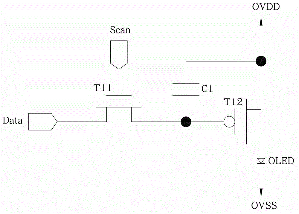
[0041] figure 1 Shows the basic principle diagram of the pixel compensation circuit in the liquid crystal panel. Reference figure 1 , The basic pixel compensation circuit is a "2T1C" architecture, where 2T is the thin film tran...


PUM


Abstract

The invention provides a pixel compensating circuit which comprises a first switch, a second switch, a third switch, a fourth switch, a fifth switch and an organic light-emitting diode, wherein a first end of the first switch is connected to a data signal; a control end of the first switch is connected to a scanning signal; a first end of the second switch is connected to reference voltage; a control end of the second switch is connected to a switching signal; a first end of the third switch is connected to first voltage; a control end of the third switch is connected to a first control signal; a first end of the fourth switch is connected to a second end of the third switch; a first end of the fifth switch is connected to a second end of the fourth switch; a control end of the fifth switch is connected to a second control signal; an anode of the organic light-emitting diode is connected to a second end of the fifth switch; and a cathode of the organic light-emitting diode is connected to second voltage. The pixel compensating circuit adopts the independent switching signal to complete write-in of the reference voltage and realizes data write-in by the complete scanning signal during a low level period, so that data pulses have adequate pulse widths to realize driving at a high frame speed, and the problem that the panel display is nonuniform is solved.

Description

technical field [0001] The invention relates to an active matrix organic light emitting diode panel, in particular to a pixel compensation circuit of the AMOLED panel. Background technique [0002] Organic light emitting diodes (Organic Light Emitting Diode, OLED) can be divided into passive matrix driving (Passive Matrix OLED, PMOLED) and active matrix driving (Active Matrix OLED, AMOLED) according to the driving method. Among them, the PMOLED does not emit light when data is not written, but only emits light during data writing. This driving method is simple in structure, low in cost, and easy to design, and is mainly suitable for small and medium-sized displays. [0003] The biggest difference between AMOLED and PMOLED is that each pixel has a capacitor to store data, so that each pixel can maintain a light-emitting state. Since the power consumption of AMOLED is significantly lower than that of PMOLED, and its driving method is suitable for the development of large-siz...

Claims


Application Information

Patent Timeline
IPC IPC(8): G09G3/32G09G3/3225
Inventor 张华罡刘立伟
Owner AU OPTRONICS CORP
Why Eureka
Try Eureka