Light emitting diode drive circuit as well as driving method and display device thereof

A technology of light-emitting diodes and driving circuits, which is applied to identification devices, static indicators, instruments, etc., can solve problems such as uneven display of the panel, and achieve the effect of improving the uneven display of the panel.

Active Publication Date: 2010-09-08
AU OPTRONICS CORP
View PDF6 Cites 3 Cited by
  • Summary
  • Abstract
  • Description
  • Claims
  • Application Information

AI Technical Summary

Problems solved by technology

[0004] The purpose of the present invention is to provide a light-emitting diode driving circuit to improve the problem of uneven panel display in the prior art
[0005] Another object of the present invention is to provide a method for driving light emitting diodes to improve the problem of uneven panel display in the prior art
[0006] Another object of the present invention is to provide a display device to improve the problem of uneven panel display in the prior art

Method used


Image

  • Light emitting diode drive circuit as well as driving method and display device thereof
  • Light emitting diode drive circuit as well as driving method and display device thereof
  • Light emitting diode drive circuit as well as driving method and display device thereof

Examples


Embodiment Construction

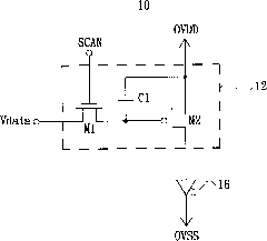
[0044] see figure 2 , which shows a schematic structural diagram of a display device related to an embodiment of the present invention. Such as figure 2As shown, the display device 20 includes a power supply device 21 and a light source 23 . Wherein, the power supply device 21 is used to provide power such as power supply potentials OVDD and OVSS; the light emitting source 23 is electrically coupled to the power supply device 21 to receive the power supply potentials OVDD and OVSS. Specifically, the light emitting source 23 includes at least one light emitting module 230 , two of which are shown in this embodiment as an example, but not limiting the present invention.

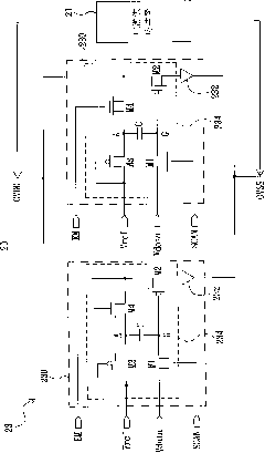
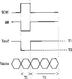
[0045] Each light emitting module 230 includes a light emitting diode such as an organic light emitting diode 232 and a light emitting diode driving circuit 234 . The LED driving circuit 234 includes a plurality of transistors M1 , M2 , M3 , M4 and a capacitor C. As shown in FIG. In this embodiment, the t...


PUM


Abstract

The invention relates to a light emitting diode drive circuit as well as a driving method and a display device thereof. The light emitting diode drive circuit comprises a first transistor, a second transistor, a third transistor, a one-way conducting element and a capacitor. The control end of the first transistor is controlled by a first signal so as to decide whether the first transistor is conducted or not; the second transistor is coupled between a power source electric potential and a light emitting diode, and the control end of the second transistor receives data signals transmitted by the first transistor when the first transistor is conducted; the control end of the third transistor is controlled by a second signal so as to decide whether the power source electric potential is transferred to the first end of the capacitor or not, and the second end of the capacitor is coupled with the control end of the second transistor; and the one-way conducting element is coupled between the first end of the capacitor and a reference signal. In addition, the reference signal makes the one-way conducting element not conducted within a certain duration due to reverse bias.

Description

technical field [0001] The invention relates to the field of display technology, and in particular to a light emitting diode driving circuit, a driving method thereof and a display device. Background technique [0002] The pixel of a light emitting diode (Light Emitting Diode, LED) display device generally uses transistors and storage capacitors to store charges to control the brightness of the light emitting diode. Produces varying degrees of shine. See figure 1 , which is a schematic diagram of a single pixel circuit of a conventional LED display device. The pixel circuit 10 is a single light-emitting module, which includes a LED driving circuit 12 and an OLED 16; the LED driving circuit 12 is used to control the brightness performance of the OLED 16, and has a two-transistor-capacitor (2T1C) structure. Specifically, the LED driving circuit 12 includes a transistor M1, a transistor M2, and a capacitor C1; the drain of the transistor M1 receives the data signal Vdata due...

Claims


Application Information

Patent Timeline
IPC IPC(8): G09G3/32G09F9/33G09G3/3233
Inventor 周佳伶吴元均张立勋
Owner AU OPTRONICS CORP
Why Eureka
Try Eureka