Semiconductor conveying equipment and taking and placing device thereof

A technology of conveying equipment and pick-and-place device, which is used in semiconductor/solid-state device manufacturing, conveyor objects, transportation and packaging, etc., can solve the problems of reduced pick-and-place chip efficiency, easy deformation, etc., to improve pick-and-place efficiency and prolong use. Longevity, the effect of reducing mechanical damage

Inactive Publication Date: 2013-03-20
QINGDAO TIANXINTONG SOFTWARE TECH
View PDF2 Cites 4 Cited by
  • Summary
  • Abstract
  • Description
  • Claims
  • Application Information

AI Technical Summary

Problems solved by technology

However, for the suction nozzle 120 made of rubber material, the larger the diameter of the suction hole 124, the easier the suction nozzle 120 is to be deformed, which in turn leads to a decrease in the efficiency of picking and placing chips of the picking and placing device 100.

Method used


Image

  • Semiconductor conveying equipment and taking and placing device thereof
  • Semiconductor conveying equipment and taking and placing device thereof
  • Semiconductor conveying equipment and taking and placing device thereof

Examples


Embodiment Construction

[0037] Below in conjunction with accompanying drawing, structural principle and working principle of the present invention are specifically described:

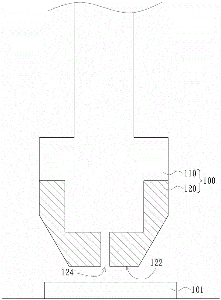
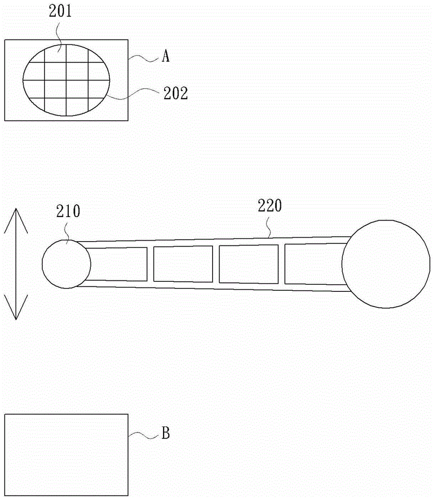
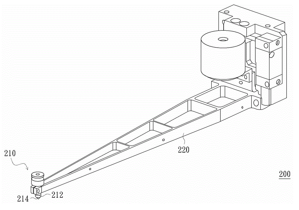
[0038] figure 2 It is a simple top view schematic diagram of semiconductor transmission equipment in an embodiment of the present invention, image 3 It is a three-dimensional schematic diagram of semiconductor transmission equipment in an embodiment of the present invention, Figure 4 Then it is a simple cross-sectional schematic diagram of the pick-and-place device in an embodiment of the present invention. Please refer to figure 2 , image 3 and Figure 4 The semiconductor transfer equipment 200 can be used to transfer the semiconductor device 201 from the temporary storage area A to the target area B. For example, the semiconductor element 201 of this embodiment is, for example, a chip, and the semiconductor transfer device 200 is, for example, a chip sorter, which is used to sort and sort the plurality of chips 201...


PUM


Abstract

The invention discloses semiconductor conveying equipment and a taking and placing device thereof. The semiconductor conveying equipment can be used for conveying a semiconductor element to a target zone from a temporary storage zone, and comprises the taking and placing device and a mechanical arm, wherein the taking and placing device comprises a suction pipe and a suction nozzle; the suction pipe of the taking and placing device is provided with a taking and placing end; the suction nozzle is arranged at the taking and placing end in a sleeving manner and provided with a taking and placing surface; in addition, the taking and placing surface is provided with a plurality of suction holes communicated with the taking and end of the suction pipe; and the mechanical arm is connected with the suction pipe of the taking and placing device, and used for driving the taking and placing device to move between the temporary storage zone and the target zone. According to the semiconductor conveying equipment, the suction nozzle with the suction holes is arranged in the taking and placing device, so that a suction force of the taking and placing device can be increased by adjusting the quantity of the suction holes and the hole diameters of the suction holes under the condition that a contact area between the suction nozzle and the semiconductor element is not changed; furthermore, the taking and placing efficiency of the taking and placing device is improved effectively; and the service life of the suction nozzle is prolonged.

Description

technical field [0001] The invention relates to a conveying device, and in particular to a semiconductor conveying device and a pick-and-place device thereof. Background technique [0002] In the current semiconductor process, after the wafer production is completed, in order to ensure the yield rate of the wafer and avoid the cost waste of the subsequent packaging process, the chip areas on the wafer are usually tested before and after the wafer is cut, and each chip is recorded. District test results. Afterwards, according to the previously recorded test results, the pick-and-place device is used to pick and store each chip on each tray for temporary storage or preparation for packaging. [0003] figure 1 It is a schematic diagram of using the existing pick-and-place device to pick and place chips. Please refer to figure 1 The pick-and-place device 100 includes a suction pipe 110 and a suction nozzle 120, wherein the suction pipe 110 is a hollow tube connected to a suc...

Claims


Application Information

Patent Timeline
Patent Type & Authority Applications(China)
IPC IPC(8): H01L21/677H01L21/683
Inventor 姜付鹏李程武传伟
Owner QINGDAO TIANXINTONG SOFTWARE TECH
Why Eureka
Try Eureka