PCB (printed circuit board) back drilling method and PCB through hole structure

A PCB board and back-drilling technology, which is applied in the direction of electrical connection formation of printed components, electrical connection of printed components, printed circuit components, etc., can solve the problems that the back-drilling process cannot be carried out, and achieve the effect of low processing cost

Inactive Publication Date: 2013-03-27
NEW H3C TECH CO LTD
View PDF2 Cites 19 Cited by
  • Summary
  • Abstract
  • Description
  • Claims
  • Application Information

AI Technical Summary

Problems solved by technology

If the trace or line plane (before back drilling) is too close to the via in the back drilling depth range, the conventional back drilling process may not work

Method used


Image

  • PCB (printed circuit board) back drilling method and PCB through hole structure
  • PCB (printed circuit board) back drilling method and PCB through hole structure
  • PCB (printed circuit board) back drilling method and PCB through hole structure

Examples


Embodiment Construction

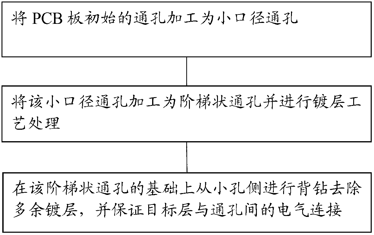
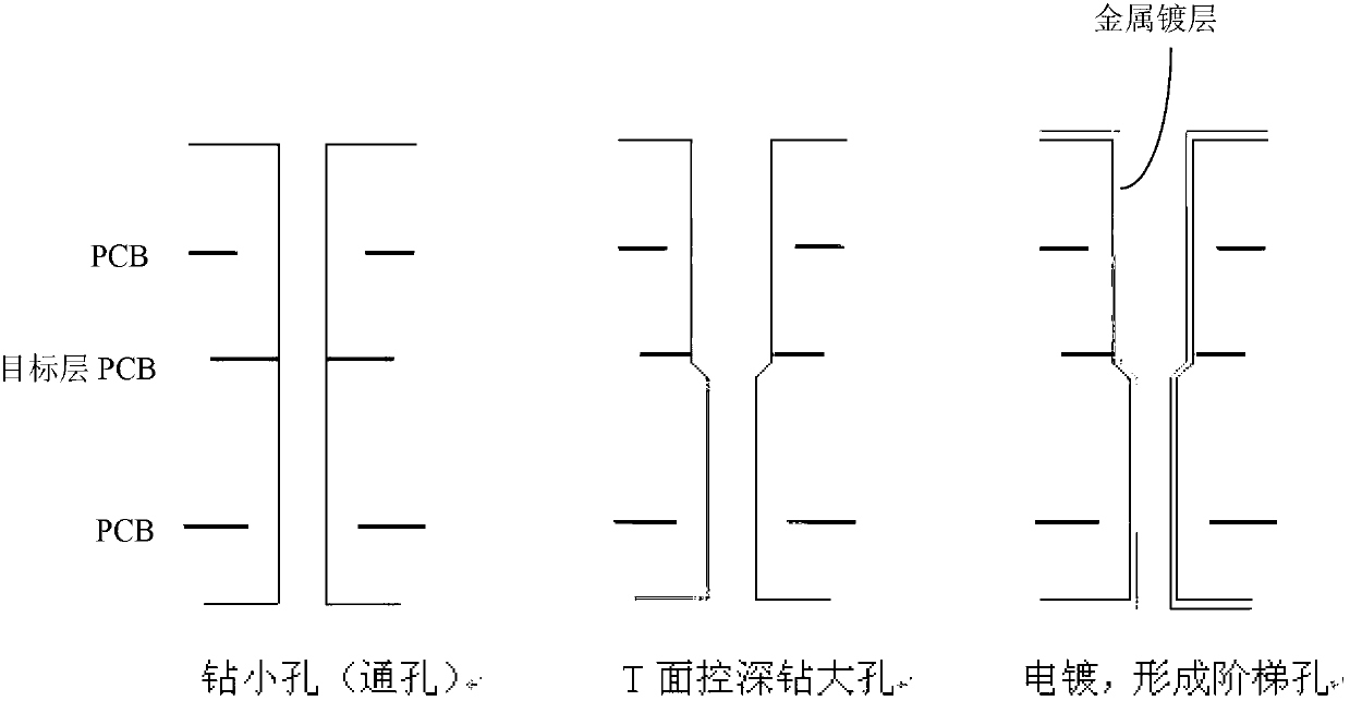
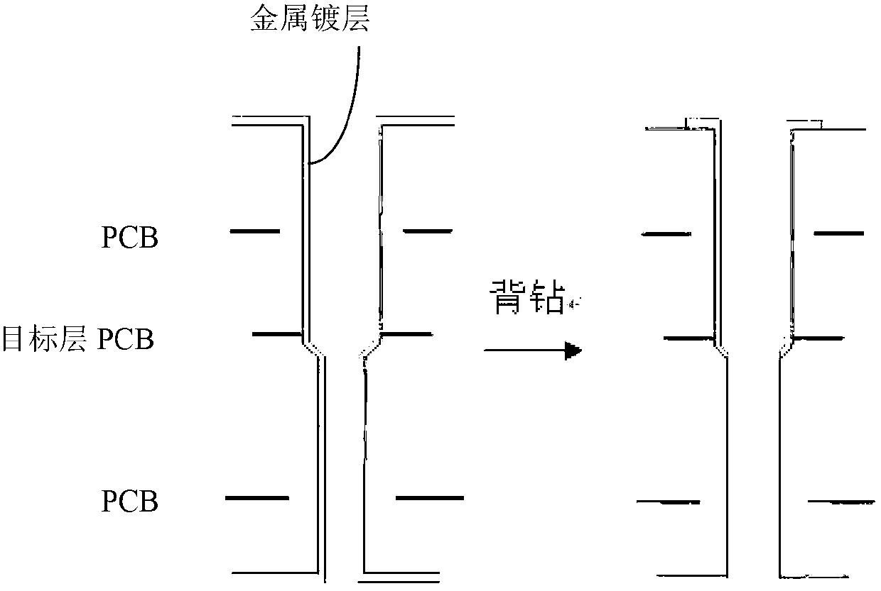
[0024] In order to achieve the purpose of the present invention, the core idea adopted by the present invention is: for the situation where the distance between the PCB trace or the plane and the through hole is insufficient, first process the initial through hole of the PCB board into a small-diameter through-hole, and then the small-diameter through-hole It is processed into a stepped through hole and processed by metal coating process. Finally, on the basis of the stepped through hole, back-drill from the small hole side to remove the excess metal coating, and ensure the coating electrical between the printed circuit of the target layer PCB board and the through hole. connect. Through the present invention, since the back-drilling process is carried out from the small hole side of the stepped hole, the diameter of the back-drilling hole becomes smaller compared with the conventional back-drilling process, and the distance from the back-drilling hole to the PCB trace or PCB p...


PUM


Abstract

Disclosed are a PCB (printed circuit board) back drilling method and a PCB through hole structure. Aiming at the problem about short distance between a PCB wiring or plane and a through hole, an original through hole in existing technical scheme is processed into a small-caliber through hole which is processed into a step-shaped through hole and subjected to metal plating process, and finally, redundant metal plated layer is removed by back drilling from the small hole on the basis of the step-shaped through hole, and a target layer and a through hole are guaranteed to be in electrical connection. By the PCB back drilling method, caliber of a back-drilled hole is smaller than that drilled by conventional back drilling method, the distance between the back-drilled hole and the PCB wiring or plane is lengthened, and meanwhile, arrangement space of the PCB wiring or plane is improved.

Description

technical field [0001] The invention relates to the technical field of communications, in particular to a PCB backdrilling method and a PCB structure. Background technique [0002] With the increase of single-layer PCB board speed, the application of PCB board back-drilling technology is more and more widely. It mainly uses the processing method of controlled depth drilling to remove the redundant metal coating in the through-holes, so as to reduce the antenna crosstalk effect and improve Signal quality and integrity. [0003] However, in order to ensure that the excess metal plating can be removed, the diameter of the back-drilled hole must be larger than the original diameter of the via, and at the same time, within the range of the back-drilled depth of the via, the PCB trace or line plane must be a certain distance away from the back-drilled hole to prevent PCB traces or circuit planes are damaged during backdrilling. If the trace or trace plane (before backdrilling) w...

Claims


Application Information

Patent Timeline
IPC IPC(8): H05K3/42H05K1/11
Inventor 朱海鸥
Owner NEW H3C TECH CO LTD
Why Eureka
Try Eureka