

Processing method for multi-way electrostatic discharge protection device
A technology of electrostatic discharge and processing method, applied in electrical components, semiconductor/solid-state device manufacturing, circuits, etc., can solve problems such as high manufacturing cost, open circuit, ESD device burst, etc., achieve low parasitic capacitance and leakage current, and reduce circuit power. The effect of reducing consumption, reducing processing difficulty and manufacturing cost
- Summary
- Abstract
- Description
- Claims
- Application Information
AI Technical Summary
Problems solved by technology
Method used
Image

Examples
Embodiment Construction
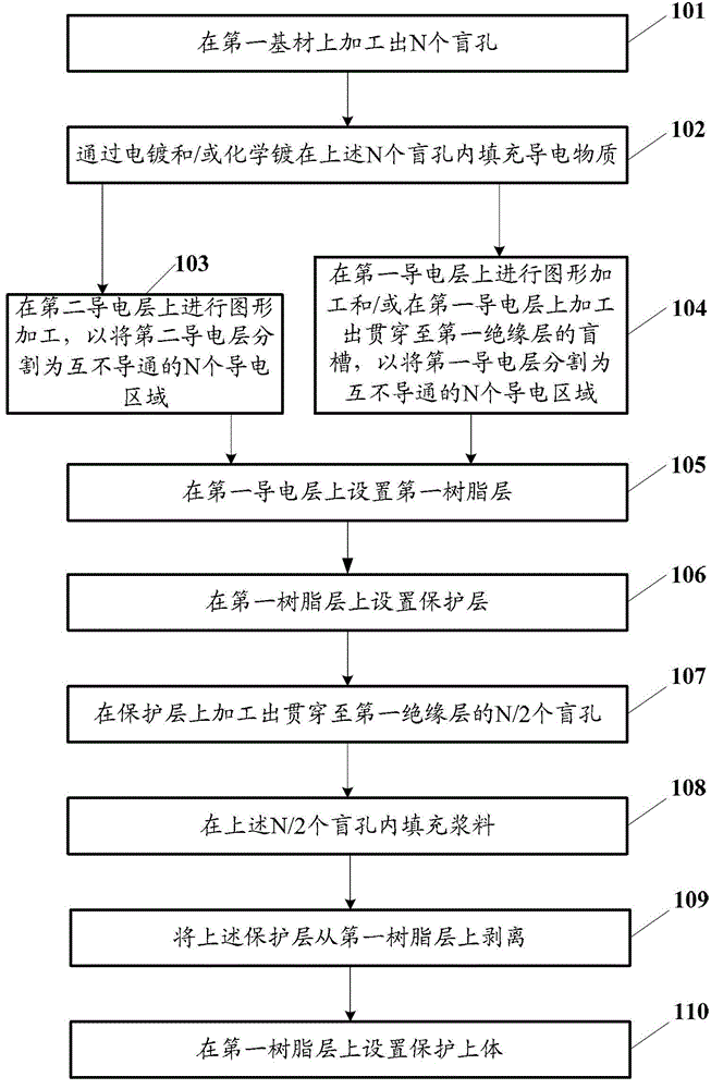
[0037] An embodiment of the present invention provides a processing method for an electrostatic discharge protection device, in order to reduce the manufacturing cost of the ESD protection device and improve the safety of the ESD protection device.
[0038]The following will clearly and completely describe the technical solutions in the embodiments of the present invention with reference to the accompanying drawings in the embodiments of the present invention. Obviously, the described embodiments are only some, not all, embodiments of the present invention. Based on the embodiments of the present invention, all other embodiments obtained by persons of ordinary skill in the art without creative efforts fall within the protection scope of the present invention.
[0039] The terms "first", "second", "third", "fourth", etc. (if any) in the description and claims of the present invention and the above drawings are used to distinguish similar objects and not necessarily Describe a p...
PUM
 Abstract
Description
Claims
Application Information