Array substrate, manufacture method of array substrate and display device

A technology of an array substrate and a manufacturing method, which is applied in the display field, can solve the problems of increasing the cost of display device products, and achieve the effects of reducing the production cost and simplifying the production steps.

Active Publication Date: 2013-04-03
BOE TECH GRP CO LTD
View PDF3 Cites 35 Cited by
  • Summary
  • Abstract
  • Description
  • Claims
  • Application Information

AI Technical Summary

Problems solved by technology

Excessive number of patterning processes will directly lead to an increase in the cost of display device products, so how to further reduce the number of patterning processes has become an issue of increasing concern

Method used


Image

  • Array substrate, manufacture method of array substrate and display device
  • Array substrate, manufacture method of array substrate and display device
  • Array substrate, manufacture method of array substrate and display device

Examples


Embodiment Construction

[0028] The following will clearly and completely describe the technical solutions in the embodiments of the present invention with reference to the accompanying drawings in the embodiments of the present invention. Obviously, the described embodiments are only some, not all, embodiments of the present invention. Based on the embodiments of the present invention, all other embodiments obtained by persons of ordinary skill in the art without making creative efforts belong to the protection scope of the present invention.

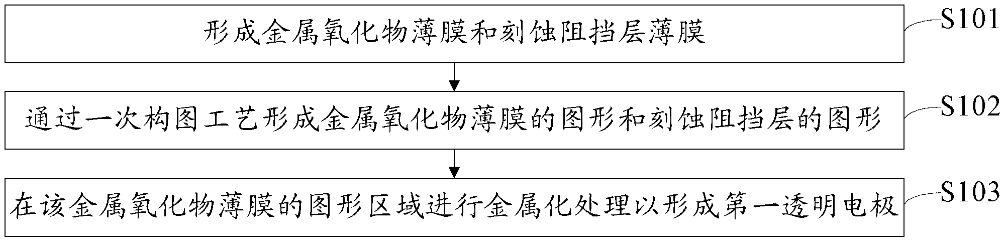
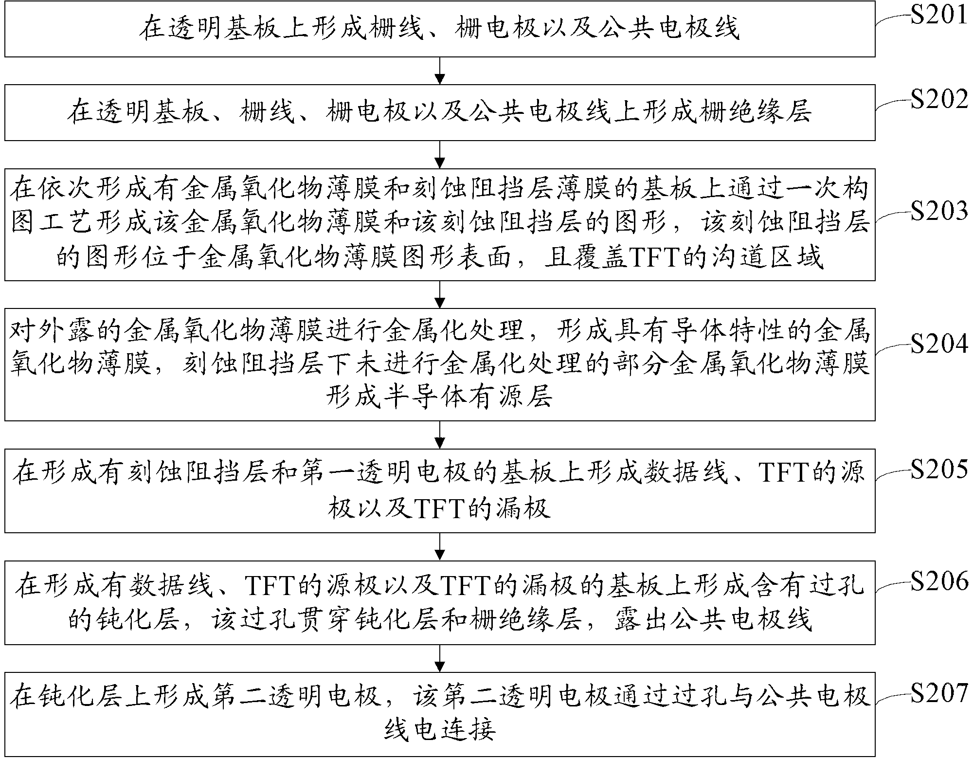
[0029] The method for manufacturing an array substrate provided by an embodiment of the present invention includes the steps of forming a thin film transistor TFT and a first transparent electrode on a transparent substrate, such as figure 1 As shown, the step of forming the first transparent electrode includes:

[0030] S101, forming a metal oxide thin film and an etching stopper thin film.

[0031] Wherein, the metal oxide thin film can be made of transpare...


PUM


Abstract

An embodiment of the invention provides an array substrate, a manufacture method of the array substrate and a display device and relates to the technical field of displaying. Times of figure composition technologies can be decreased in the array substrate manufacture process, and production cost of products can be effectively reduced. The manufacture method comprises the steps of forming a thin film transistor (TFT) and forming a first transparent electrode. The step of forming the first transparent electrode includes the steps of forming a metal oxide film, forming a barrier layer film and forming an etching barrier layer film. A figure of the metal oxide film and a figure of the etching barrier layer film are formed through one-time figure composition technologies. Metallization processing is performed in a figure region of a metal oxide film to form the first transparent electrode. The manufacture method is used for manufacture of the display device.

Description

technical field [0001] The present invention relates to the field of display technology, in particular to an array substrate, a manufacturing method thereof, and a display device. Background technique [0002] With the continuous development of TFT-LCD (Thin Film Transistor Liquid Crystal Display, Thin Film Transistor Liquid Crystal Display) display technology, more and more new technologies are constantly being proposed and applied. TFT-LCD based on ADS (ADvanced Super Dimension Switch, AD-SDS, referred to as ADS, Advanced Super Dimension Field Switching Technology) mode has attracted more and more people's attention due to its low power consumption, wide viewing angle and other characteristics. [0003] ADS technology mainly forms a multi-dimensional electric field through the electric field generated by the edge of the slit electrode in the same plane and the electric field generated between the slit electrode layer and the plate electrode layer, so that all aligned liqui...

Claims


Application Information

Patent Timeline
Patent Type & Authority Applications(China)
IPC IPC(8): H01L21/77H01L27/02
Inventor 崔承镇金熙哲宋泳锡刘圣烈
Owner BOE TECH GRP CO LTD
Why Eureka
Try Eureka