Method for making MOS having light doped drain electrode

A technology of oxide semiconductor and lightly doped drain, which is applied in semiconductor/solid-state device manufacturing, electrical components, circuits, etc., and can solve problems such as narrow process range, difficult control, and unfavorable actual production

Active Publication Date: 2005-09-21
AU OPTRONICS CORP
View PDF0 Cites 18 Cited by
  • Summary
  • Abstract
  • Description
  • Claims
  • Application Information

AI Technical Summary

Problems solved by technology

In the above-mentioned thin film transistor manufacturing method that reduces the number of photomasks used, although the number of photomasks used can be reduced, the most critical and difficult part of the above technology is that the photoresi

Method used


Image

  • Method for making MOS having light doped drain electrode
  • Method for making MOS having light doped drain electrode
  • Method for making MOS having light doped drain electrode

Examples


Embodiment Construction

[0028] The invention provides a metal oxide semiconductor manufacturing method with a lightly doped drain, which can effectively reduce the number of photomasks used in the thin film transistor process, reduce process complexity and increase yield. The metal oxide semiconductor with lightly doped drain is applied to a thin film transistor liquid crystal display. The following is an example of a preferred embodiment of the method for fabricating a lightly doped drain metal oxide semiconductor according to the present invention, which is described in detail with reference to the accompanying drawings:

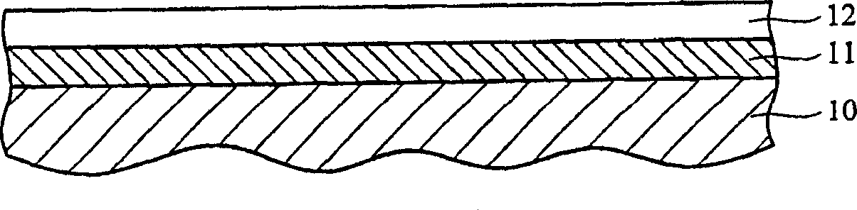
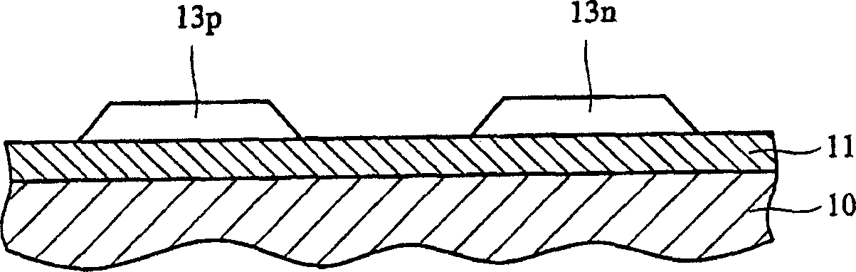
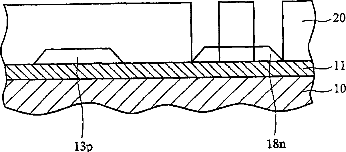
[0029] First, see Figure 3a , providing a substrate 200, which may be, for example, a suitable substrate for a liquid crystal display, and the substrate 200 includes a P-type metal oxide semiconductor region P and a lightly doped drain region LDD. Next, a buffer layer 202 and a semiconductor layer are sequentially formed on the substrate 200 . Next, using a first photomask and...


PUM


Abstract

This invention provides a method for making MOS with light doped drain electrode, which contains defining grid, P-type ion heavy doped area and N-type ion light doped area using one photo mask, and can also defining contact window and N-type ion heavy doped area using another photo mask, only six photo masks are needed for completing the process of light doped drain electrode film transistor, so the production speed and yield are increased.

Description

technical field [0001] The invention relates to a thin film transistor and a manufacturing method thereof, in particular to a thin film transistor capable of reducing the number of photomasks used in the process and a manufacturing method thereof. Background technique [0002] Thin film transistor (thin film transistor, TFT) is an active element commonly used in active matrix type flat panel display, used to drive active matrix type liquid crystal display (active matrix type liquid crystal display), active organic electroluminescence display (active matrix type organicelectroluminescent display), image sensor and other devices. Generally, thin film transistors can be classified into polysilicon thin film transistors and amorphous silicon thin film transistors according to the composition of the semiconductor silicon layer of the thin film transistors. [0003] In order to achieve high-precision element and pixel arrangement, polysilicon has gradually replaced amorphous sili...

Claims


Application Information

Patent Timeline
IPC IPC(8): H01L21/336
Inventor 颜士益
Owner AU OPTRONICS CORP
Why Eureka
Try Eureka