Method for manufacturing semiconductor device

一种半导体、器件的技术,应用在从晶圆载体(wafer carrier)上分离半导体器件领域,能够解决消耗时间总产量、制约瓶颈等问题

Active Publication Date: 2013-04-10
INFINEON TECH AG
View PDF7 Cites 7 Cited by
  • Summary
  • Abstract
  • Description
  • Claims
  • Application Information

AI Technical Summary

Problems solved by technology

But such a process is time consuming and can become a limiting bottleneck for overall throughput

Method used


Image

  • Method for manufacturing semiconductor device
  • Method for manufacturing semiconductor device
  • Method for manufacturing semiconductor device

Examples


Embodiment Construction

[0044] The making and using of various embodiments are described in detail below. It should be appreciated, however, that the present invention provides many applicable inventive concepts, which can be embodied in various ways depending on the particular situation. The specific embodiments described herein are just to illustrate the specific ways of realizing and utilizing the present invention, and do not limit the scope of the present invention.

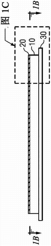
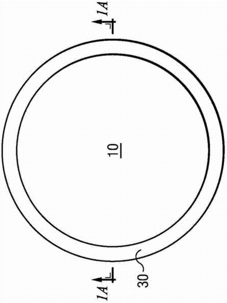
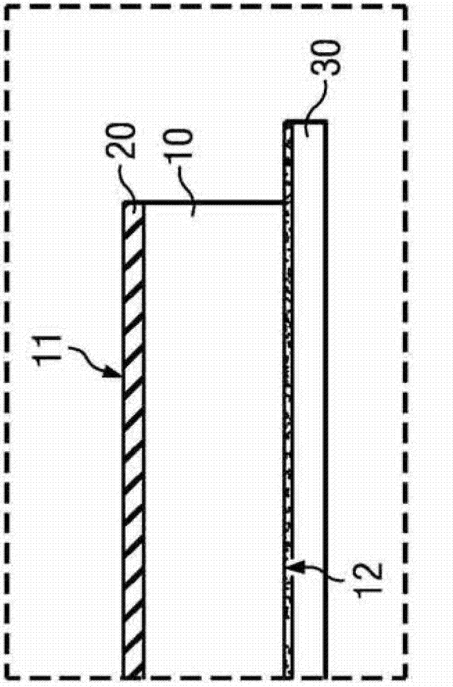
[0045] A method of quickly removing a semiconductor die attached to a wafer frame (frame with adhesive foil) or a carrier will be described using FIGS. 1-10, 17-18, 19-20 according to an embodiment of the invention. will use Figure 11 The carbon dioxide snow injection used in the embodiment of the present invention will be described. An embodiment of removing, for example, a defective die from a frame with an adhesive foil will be explained using FIG. 12 . Embodiments of the present invention for removing packaged semiconductor ...


PUM


Abstract

In accordance with an embodiment of the present invention, a semiconductor device is manufactured by arranging a plurality of semiconductor devices on a frame with an adhesive foil. The plurality of semiconductor devices is attached to the adhesive foil. The plurality of semiconductor devices is removed from the frame with the adhesive foil using a carbon dioxide snow jet and / or a laser process.

Description

technical field [0001] The present invention relates generally to a method, and more particularly to a method of separating semiconductor devices from a wafer carrier. Background technique [0002] Semiconductor devices are used in many electronic and other applications. Semiconductor devices may include integrated circuits formed on semiconductor wafers. Alternatively, semiconductor devices may be formed as monolithic devices, such as discrete devices. Semiconductor devices are formed on a semiconductor wafer by placing various material films on the semiconductor wafer, patterning the material films, doping selected regions of the semiconductor wafer, and the like. [0003] In traditional semiconductor manufacturing processes, a large number of semiconductor devices are fabricated on a single wafer. After the device-level and interconnect-level manufacturing processes are completed, the semiconductor devices on the wafer are separated. For example, wafers can be diced a...

Claims


Application Information

Patent Timeline
Patent Type & Authority Applications(China)
IPC IPC(8): H01L21/78H01L21/683B23K26/36
CPCH01L23/3107H01L21/561H01L21/565H01L21/568H01L2924/0002H01L21/67092H01L21/67144H01L21/6836H01L2221/68322H01L2221/68327H01L2221/6834H01L2221/68368H01L2221/68381H01L2924/00H01L21/78H01L21/50H01L21/67H01L21/683
Inventor 塞巴斯蒂安·贝恩里德阿道夫·科勒斯特凡·马滕斯马蒂亚斯·沃佩尔
Owner INFINEON TECH AG
Why Eureka
Try Eureka