flash interface circuit
A technology of interface circuit and FLASH memory, applied in information storage, static memory, instrument, etc., can solve the problems of few non-contact smart cards, small and large FLASH area, etc.
- Summary
- Abstract
- Description
- Claims
- Application Information
AI Technical Summary
Problems solved by technology
Method used
Image

Examples
Embodiment Construction
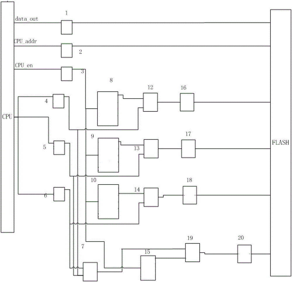
[0015] See attached figure 1 , a FLASH interface circuit, which is installed between the CPU and the FLASH memory, it includes: data register 1, read and write address register 2, enable signal generating circuit 3, width configuration register A4, width configuration register B5, width configuration register C6, comparison selection circuit 7, counter A8, counter B9, counter C10, comparison circuit A12, comparison circuit B13, comparison circuit C14, counter D15, pulse generator A16, pulse generator B17, pulse generator C18, comparison circuit D19 and Pulse generator D20;
[0016] Its connection relationship is: the data register 1 and the read-write address register 2 are respectively connected between the CPU and the FLASH memory; The counter C10 and the counter D15 are connected; one end of the width configuration register A4 is connected with the CPU, and the other end is divided into two paths, one path is connected with the comparison selection circuit 7, and the other...
PUM
 Abstract
Description
Claims
Application Information