Supercharge Your Innovation With Domain-Expert AI Agents!

Method for detecting epitaxial silicon defects

A technology of epitaxial silicon and defects, applied in measuring devices, material analysis through electromagnetic means, instruments, etc., can solve problems such as difficult to ensure accuracy, surface distribution detection of small defects, and silicon wafers can not continue to be used, etc., to achieve quantitative Determine the effect of degree and location

Inactive Publication Date: 2013-04-24
SHANGHAI HUAHONG GRACE SEMICON MFG CORP
View PDF7 Cites 3 Cited by
  • Summary
  • Abstract
  • Description
  • Claims
  • Application Information

AI Technical Summary

Problems solved by technology

Although this method is more intuitive and clear, there are still some unavoidable problems.
First of all, acid corrosion defect monitoring has high requirements for operating technicians, otherwise it is difficult to ensure very accurate
Secondly, the acid etching method belongs to the destructive measurement of silicon wafers, and the silicon wafers will not be able to continue to be used after completion
In addition, another problem faced by the acid etching method is that it is impossible to detect the surface distribution of a small number of defects.

Method used


Image

  • Method for detecting epitaxial silicon defects
  • Method for detecting epitaxial silicon defects
  • Method for detecting epitaxial silicon defects

Examples


Embodiment Construction

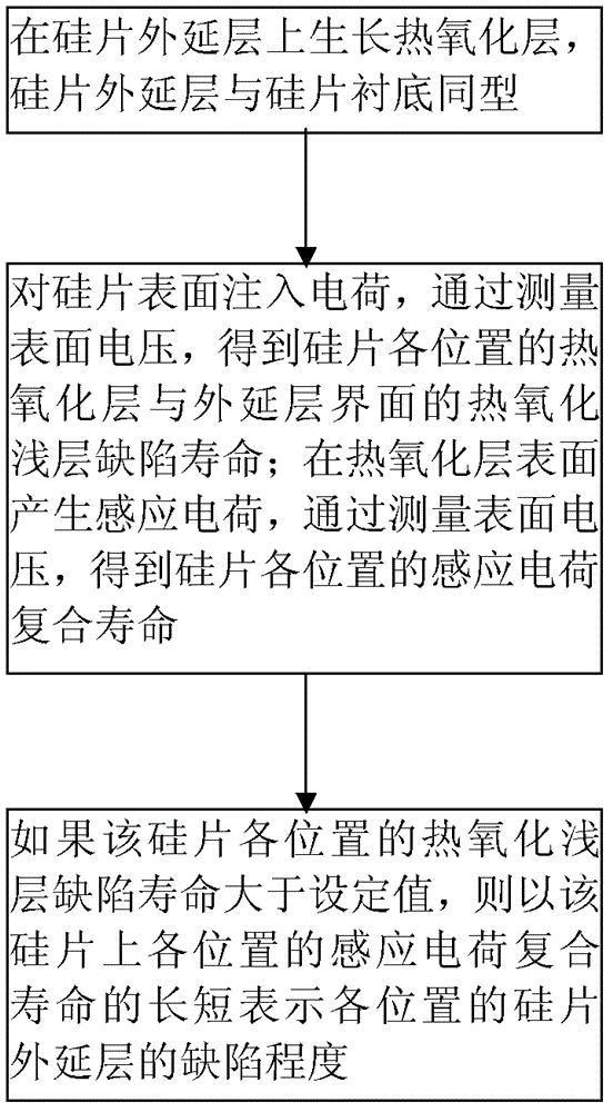
[0017] An embodiment of the method for detecting epitaxial silicon defects of the present invention is as follows: figure 1 as shown, including the following steps:

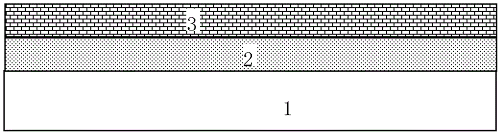
[0018] 1. The thermal oxide layer 3 is grown on the silicon wafer epitaxial layer 2, and the silicon wafer epitaxial layer 2 is the same type as the silicon wafer substrate 1 (both N-type or P-type), such as figure 2 shown;

[0019] 2. Inject charges into the surface of the silicon wafer, and then measure the surface voltage to obtain the thermally oxidized shallow layer defect life of the interface between the thermally oxidized layer and the epitaxial layer at each position of the silicon wafer;

[0020] The induced charge is generated on the surface of the thermal oxide layer, and the recombination life of the induced charge at each position of the silicon wafer is also obtained by measuring the surface voltage;

[0021] 3. If the defect lifetime of the thermally oxidized shallow layer at each position of t...


PUM

PropertyMeasurementUnit
thicknessaaaaaaaaaa

Abstract

The invention discloses a method for detecting epitaxial silicon defects. The method comprises the following steps of: growing thermal oxidation layers on an epitaxial layer of a silicon slice, wherein the epitaxial layer of the silicon slice and a silicon slice substrate are in a same type; injecting charges to the surface of the silicon slice, and measuring a surface voltage, thus obtaining the defect service life of a thermal oxidation layer on each part of the silicon slice and shallow thermal oxidation layers of an epitaxial layer interface; generating induced charges on the surface of the thermal oxidation layer, thus obtaining the recombination service life of the induced charge of each part of the silicon slice in a similar way; and if the defect service life of the shallow thermal oxidation layer of each part of the silicon slice is greater than a setting value, indicating the defect degree of the epitaxial layer of each part of the silicon slice by the length of the recombination service life of the induced charge of each part of the silicon slice. The method for detecting the epitaxial silicon defects provided by the invention can make a qualitative and quantitative judgment on the degrees and the positions of the defects of the epitaxial layers of the silicon slice, and thus the judgment is more exact and complete.

Description

technical field [0001] The present invention relates to semiconductor technology, in particular to a method for detecting epitaxial silicon defects. Background technique [0002] The epitaxial process is very important in semiconductors. Various high-voltage devices and high-frequency devices need to use the epitaxial process as a buried layer or to improve the breakdown voltage of the collector of bipolar devices. Since the epitaxial layer is widely used in many key processes of the device, the quality of the epitaxial layer film is very important. [0003] The quality of epitaxial thin films usually encounters many problems, such as particles, defects and so on. Among them, the detection of defects is a reflection of the lattice level and the same substance as the silicon wafer substrate, so it is difficult to solve it by ordinary optical measurement methods. Usually, the evaluation of defects is mainly through acid etching after thick epitaxial growth, and then confirme...

Claims


Application Information

Patent Timeline
Patent Type & Authority Applications(China)
IPC IPC(8): G01N27/61
Inventor 孙勤高杏钱志刚
Owner SHANGHAI HUAHONG GRACE SEMICON MFG CORP
Features
  • R&D
  • Intellectual Property
  • Life Sciences
  • Materials
  • Tech Scout
  • Unparalleled Data Quality
  • Higher Quality Content
  • 60% Fewer Hallucinations
Learn More