Method for processing patterns in blind slot of printed circuit board

A processing method and a technology for printed boards, which are applied in the manufacture of printed circuits, removal of conductive materials by chemical/electrolytic methods, and printed circuits. Solve problems such as hole metallization, and achieve the effect of improving product qualification rate and improving the control of glue overflow

Active Publication Date: 2013-05-01
GCI SCI & TECH
View PDF3 Cites 27 Cited by
  • Summary
  • Abstract
  • Description
  • Claims
  • Application Information

AI Technical Summary

Problems solved by technology

When it is necessary to make metallized through holes and circuit patterns at the bottom of the blind slot, the metallization of the side wall of the blind slot cannot be processed according to the conventional process, and the problem of forming a network between the line and the hole at the bottom of the blind slot cannot be effectively solved after the hole is metallized
In addition, it is difficult to control the glue overflow of the prepreg on the side of the bottom of the blind groove, and there are problems of excessive glue overflow or gaps, which require manual repairs, which cannot guarantee the pass rate of the product, and the labor cost is high

Method used


Image

  • Method for processing patterns in blind slot of printed circuit board
  • Method for processing patterns in blind slot of printed circuit board
  • Method for processing patterns in blind slot of printed circuit board

Examples


Embodiment Construction

[0025] The following will clearly and completely describe the technical solutions in the embodiments of the present invention with reference to the accompanying drawings in the embodiments of the present invention. Obviously, the described embodiments are only some, not all, embodiments of the present invention. Based on the embodiments of the present invention, all other embodiments obtained by persons of ordinary skill in the art without creative efforts fall within the protection scope of the present invention.

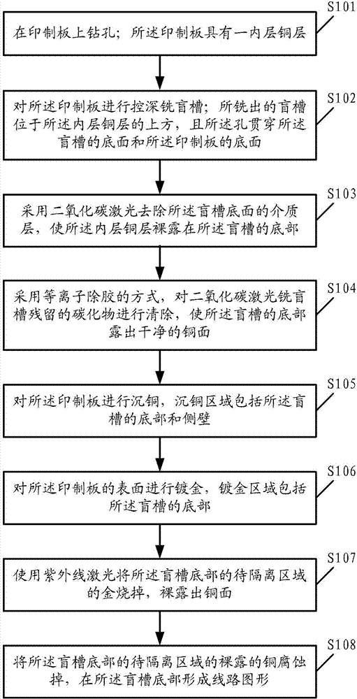
[0026] see figure 1 , is a schematic flowchart of an embodiment of a method for processing patterns in blind slots of printed boards provided by the present invention.

[0027] An embodiment of the present invention provides a method for processing a pattern in a blind slot of a printed board, comprising the following steps:

[0028] S101. Drill holes on the printed board; the printed board has an inner copper layer.

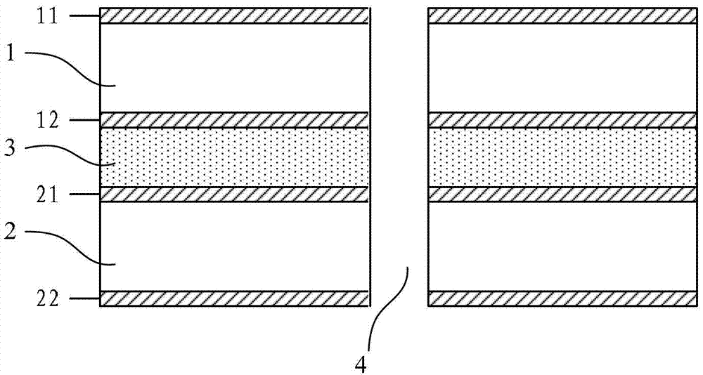
[0029] In one embodiment, as image 3 As sh...


PUM


Abstract

The invention discloses a method for processing patterns in a blind slot of a printed circuit board. The method comprises the following steps of drilling a hole in the printed circuit board; forming an inner copper layer on the printed circuit board; milling the blind slot with controlled depth on the printed circuit board; exposing the inner copper layer at the bottom of the blind slot; carrying out electroless copper plating on the printed circuit board, wherein the electroless copper plating areas comprise the bottom and the side walls of the blind slot; plating gold on the surface of the printed circuit board, wherein the gold plating area comprises the bottom of the blind slot; using an ultraviolet ray to burn the gold on the area to be isolated at the bottom of the blind slot, and exposing the copper surface; and corroding the exposed copper on the area to be isolated at the bottom of the blind slot, so as to form a circuit pattern at the bottom of the blind slot. The method disclosed by the embodiment of the invention has the advantages that the metallizing of the side wall of the blind slot is realized, the metallic through hole and the circuit pattern are manufactured at the bottom of the blind slot, and the qualified rate of the pattern is improved.

Description

technical field [0001] The present invention relates to the technical field of printed circuit board (Printed Circuit Board, PCB for short) manufacturing technology, in particular to a method for processing graphics in blind slots of printed circuit boards. Background technique [0002] With the rapid development of communication and telecommunications industries, the volume of PCB boards in electronic equipment is getting smaller and smaller, and the circuit density is getting higher and higher. In order to meet the performance requirements of all aspects of design and assembly, a blind groove design structure is produced. [0003] At present, the circuit board manufacturing industry mainly adopts the blind groove slotting process to make blind grooves. The specific process is: prepreg and sub-core board gong groove → making graphics on the inner layer of the mother core board → pressing the sub-core board, prepreg and mother core board together → Make outer layer circuit ...

Claims


Application Information

Patent Timeline
Patent Type & Authority Applications(China)
IPC IPC(8): H05K3/00H05K3/06
Inventor 唐有军杨泽华关志锋任代学刘国汉
Owner GCI SCI & TECH
Why Eureka
Try Eureka