Chip validation method and device and system based on field programmable gate array (FPGA)

A verification method and chip technology, applied in the direction of instruments, static indicators, etc., can solve the problems of low verification coverage, inability to objectively and accurately realize automatic verification, etc., and achieve the effect of improving the coverage.

Active Publication Date: 2013-05-08
ANYKA (GUANGZHOU) MICROELECTRONICS TECH CO LTD
View PDF3 Cites 15 Cited by
  • Summary
  • Abstract
  • Description
  • Claims
  • Application Information

AI Technical Summary

Problems solved by technology

[0008] The purpose of the embodiments of the present invention is to provide an FPGA-based chip verification method, which aims to solve the problem that the existing verification method has low verification coverage and cannot objectively and accurately realize automatic verification.

Method used


Image

  • Chip validation method and device and system based on field programmable gate array (FPGA)
  • Chip validation method and device and system based on field programmable gate array (FPGA)
  • Chip validation method and device and system based on field programmable gate array (FPGA)

Examples


Embodiment Construction

[0026] In order to make the object, technical solution and advantages of the present invention clearer, the present invention will be further described in detail below in conjunction with the accompanying drawings and embodiments. It should be understood that the specific embodiments described here are only used to explain the present invention, not to limit the present invention.

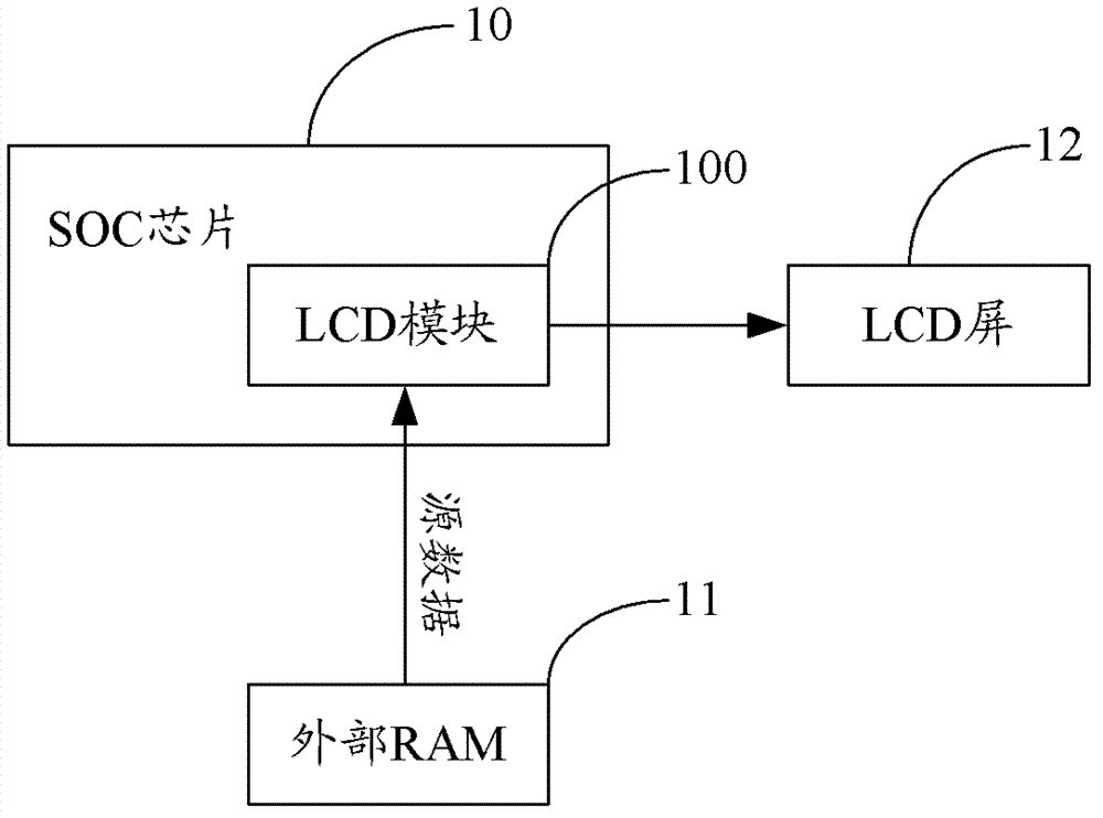
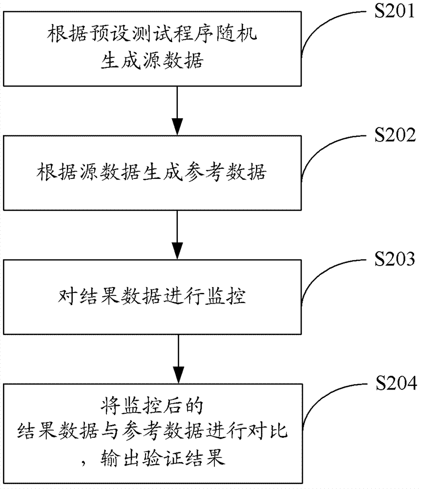
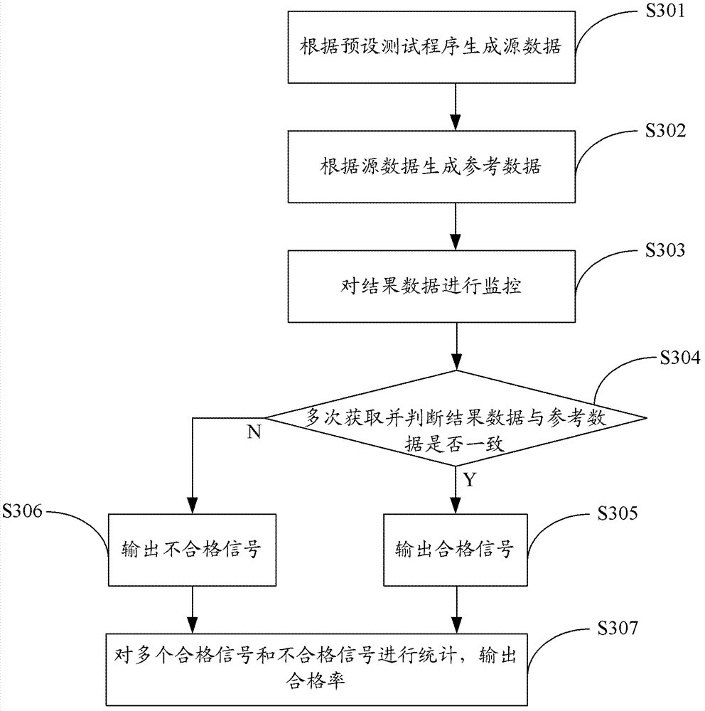
[0027] The embodiment of the present invention verifies the LCD module by randomly generating source data, and uses a monitoring unit to compare the result data with reference data, thereby realizing objective and accurate automatic verification and improving verification coverage.

[0028] figure 2 The implementation flow of the FPGA-based chip verification method provided by the first embodiment of the present invention is shown. For the convenience of description, only the parts related to the present invention are shown.

[0029] As an embodiment of the present invention, this FPGA-based chip...


PUM


Abstract

The invention belongs to the field of chip validation and provides a chip validation method and a device and a system based on field programmable gate array (FPGA). The chip validation method based on the FPGA comprises the steps that source data are generated randomly according to a preset test program, the source data are used for generating result data after being processed in a displaying mode through a liquid crystal display (LCD) module to be tested, reference data are generated according to the source data, the result data are monitored, the result data after being monitored are compared with the reference data, and verification results are output. According to the chip validation method and the device and the system based on the FPGA, the LCD module is verified by the source data generated randomly, coverage rate of the validation is improved, a monitoring unit is adopted to replace an LCD screen to monitor the result data output by the LCD module and to compare the result data with the reference data, automatic validation is achieved, objectivity of the validation is improved, and precision of the validation is also improved.

Description

technical field [0001] The invention belongs to the field of chip verification, and in particular relates to an FPGA-based chip verification method, device and system. Background technique [0002] In a system on chip (SOC, system on chip) multimedia processing chip, a liquid crystal display (LCD) module is generally integrated to control the display of a liquid crystal display (LCD, Liquid Crystal Display) in a multimedia device, and its display effect directly affects the The promotion and application of multimedia equipment, so it is particularly important to provide a complete LCD module. [0003] The quality of LCD modules is generally guaranteed by various verification methods, among which Field Programmable Gate Array (FPGA, Field Programmable Gate Array) verification is a relatively common and important verification method. In the existing FPGA verification environment, LCD modules The verification method is: at first, the video data to be displayed is placed in the...

Claims


Application Information

Patent Timeline
Patent Type & Authority Applications(China)
IPC IPC(8): G09G3/00
Inventor 王恒军胡胜发
Owner ANYKA (GUANGZHOU) MICROELECTRONICS TECH CO LTD
Why Eureka
Try Eureka