8-bit semiconductor storage unit, manufacturing method and storage unit array thereof

An 8-bit, storage unit technology, used in semiconductor/solid-state device manufacturing, semiconductor devices, information storage, etc.

Active Publication Date: 2015-11-25
SEMICON MFG INT (SHANGHAI) CORP
View PDF6 Cites 0 Cited by
  • Summary
  • Abstract
  • Description
  • Claims
  • Application Information

AI Technical Summary

Problems solved by technology

[0005] Although floating gate and SONOS memory cells have excellent storage performance, the storage capacity of conventional 1-bit memory cells can no longer meet people's requirements for memory miniaturization and large storage capacity. In order to better adapt to practical applications , around the improvement of semiconductor memory storage performance, especially the improvement of its storage density has been the focus of researchers

Method used


Image

  • 8-bit semiconductor storage unit, manufacturing method and storage unit array thereof
  • 8-bit semiconductor storage unit, manufacturing method and storage unit array thereof
  • 8-bit semiconductor storage unit, manufacturing method and storage unit array thereof

Examples


Embodiment Construction

[0055] In order to make the object, technical solution and advantages of the present invention clearer, the present invention will be further described in detail below with reference to the accompanying drawings and examples.

[0056] In order to clearly describe the structure and method of the present invention, the meanings of the following terms are defined here:

[0057] "Relative" means that the two are symmetrical about the center of the symmetry point, and "adjacent" means that the two are close to each other.

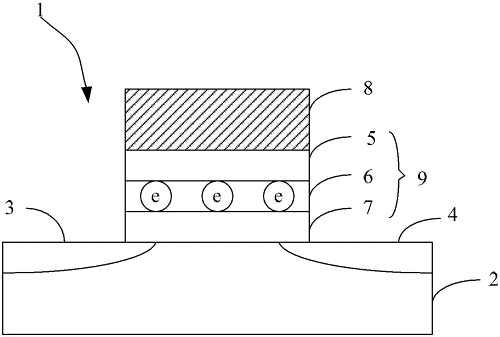
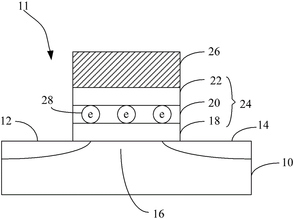
[0058] The present invention provides an 8-bit memory cell, which includes a source region and a drain region, a semiconductor fin, a gate region, and an active region and a gate region disposed on a semiconductor substrate. , A charge storage recombination layer having a charge trapping layer.

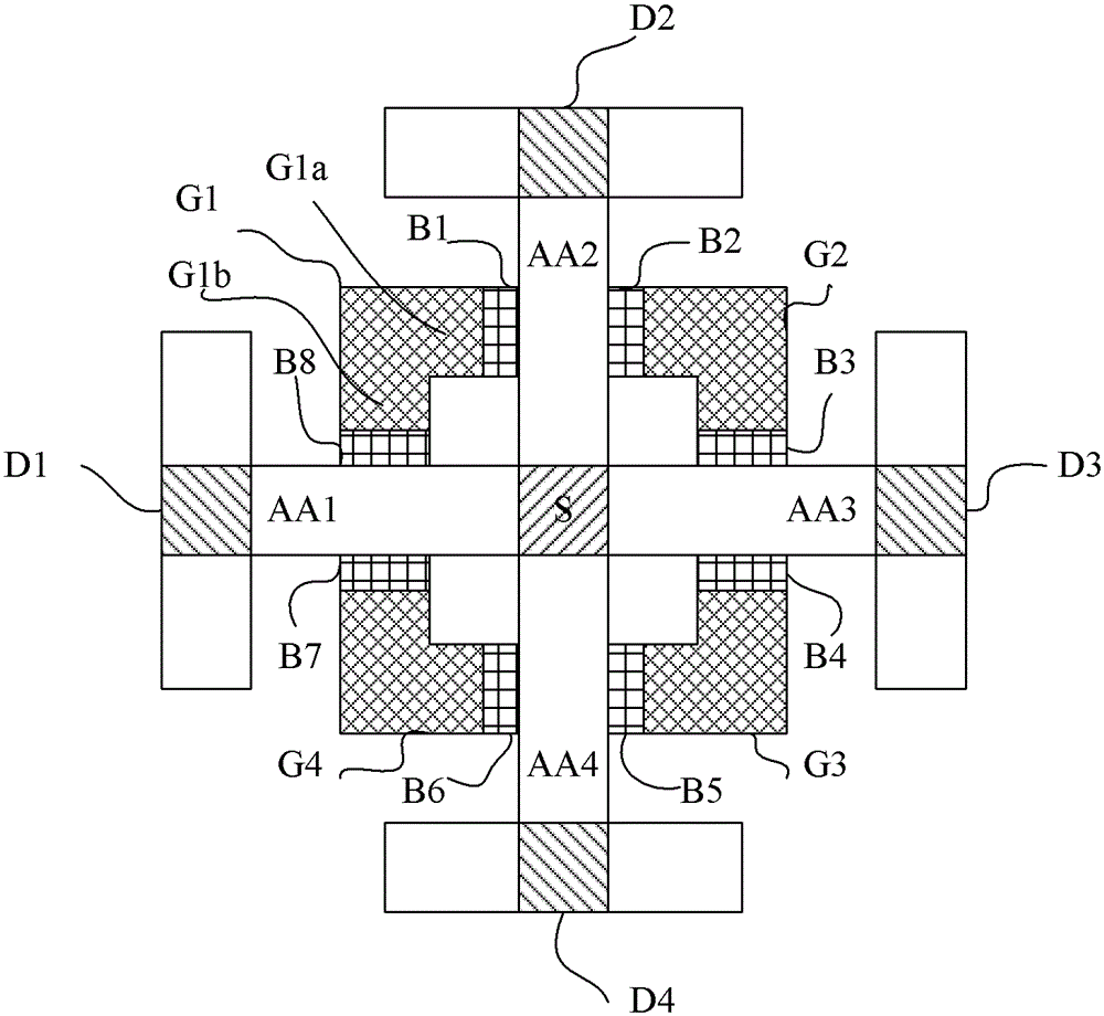
[0059] image 3 It is a top view of the semiconductor storage unit of the present invention, such as image 3 The semiconductor storage unit shown includes one sourc...


PUM


Abstract

The invention provides an 8-bit semi-conductor storage unit, a manufacture method and a storage unit array of the 8-bit semi-conductor storage unit. The 8-bit semi-conductor storage unit comprises a source area, four drain areas, four grid areas, four strip-shaped semi-conductor fins and eight charge storage composite layers, wherein four drains are symmetrically arranged outside a source electrode, one strip-shaped semi-conductor fin with a channel region is arranged between each drain electrode and the source electrode, each drain electrode is arranged between each two adjacent strip-shaped semi-conductor fins, and each grid are in contact with the channel region between the semi-conductor fins at two sides of the corresponding grid through the charge storage composite layers with charge capture layers. By means of the novel structure, 8-bit storage of the storage unit is ingeniously achieved, and storage density of the storage unit is further improved.

Description

technical field [0001] The invention relates to the field of semiconductor memory, in particular to an 8-bit semiconductor memory unit, a manufacturing method and a memory unit array thereof. Background technique [0002] As a type of semiconductor memory, a polysilicon floating gate memory cell structure (FloatingGate) has been widely used. Generally, a 1-bit polysilicon floating gate memory cell structure 1 includes a semiconductor substrate 2, an active region including a source 3 and a drain 4 is formed on the semiconductor substrate, and a blocking oxide layer 5, a floating The gate 6, the tunnel oxide layer 7 and the control gate 8, the blocking oxide layer 5, the floating gate 6, and the tunnel oxide layer 7 form a charge storage composite layer 9, such as figure 1 shown. When programming, a higher programming voltage is applied to the drain 4 and the control gate 8, and the source 3 is grounded. In this way, a large number of electrons flow from the source 3 to th...

Claims


Application Information

Patent Timeline
Patent Type & Authority Patents(China)
IPC IPC(8): H01L27/115H01L29/792H01L21/8247G11C11/413
Inventor 凌龙张传宝陈荣堂邓霖黄军
Owner SEMICON MFG INT (SHANGHAI) CORP
Why Eureka
Try Eureka