Gate material, gate unit and memory device structure

A technology of storage devices and gating tubes, applied in the direction of electrical components, etc., can solve the problems of complex material components, poor fatigue performance, and small turn-on current of the gating tube, and achieve simple and non-toxic materials, good fatigue performance, and low turn-on current big effect

Active Publication Date: 2022-01-28
SHANGHAI INST OF MICROSYSTEM & INFORMATION TECH CHINESE ACAD OF SCI
View PDF0 Cites 0 Cited by
  • Summary
  • Abstract
  • Description
  • Claims
  • Application Information

AI Technical Summary

Problems solved by technology

[0004] In view of the above-mentioned shortcomings of the prior art, the purpose of the present invention is to provide a gate material, a gate unit and a storage device structure, which are used to solve the problem of complex components and high toxicity of the existing gate materials. , small turn-on current, large leakage current, small gating ratio and poor fatigue performance, etc.

Method used


Image

  • Gate material, gate unit and memory device structure
  • Gate material, gate unit and memory device structure
  • Gate material, gate unit and memory device structure

Examples


Embodiment 1

[0047] This embodiment provides a gate material, which is a compound including at least Ge (germanium) and S (sulfur), and the general chemical formula of the gate material is (Ge x S 1-x ) 1-y m y , wherein M includes doping materials, and 0.1≤x≤0.9, 0≤y≤0.5.

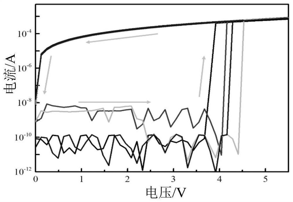
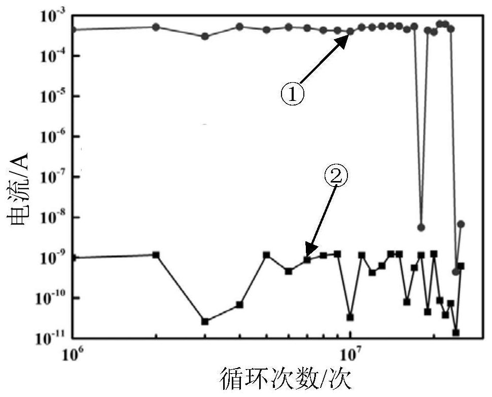
[0048] The value of y in the general chemical formula of the gating tube material can be 0, that is, the gating tube material does not contain doping materials, that is, the gating tube material is a compound including Ge and S at this time , the general chemical formula of the gating tube material is Ge x S 1-x , 0.1≤x≤0.9. The material of the gate tube at this time has an opening current I when it is used for the gate tube unit on Large, leakage current I off Small, gate ratio (I on / I off ) large, good thermal stability, simple material and non-toxic.

[0049] The value of y in the general chemical formula of the gating tube material may not be zero, that is, the gating tube material contains a doping mate...

Embodiment 2

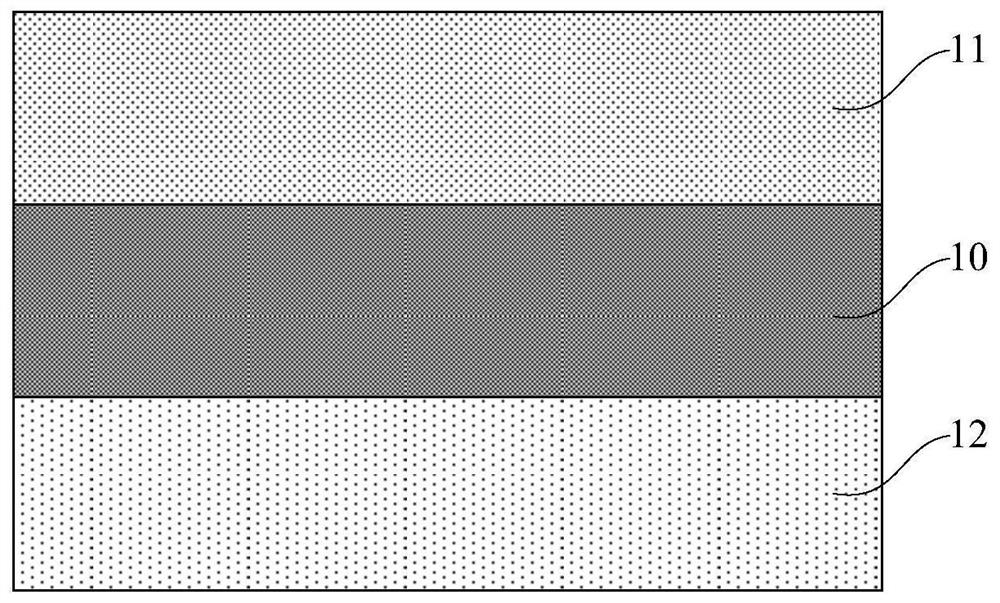
[0058] see figure 1 , the present invention also provides a gating tube unit, the gating tube unit includes: a gating tube material layer 10, a first electrode 11 and a second electrode 12; wherein,

[0059] The gate material layer 10 includes the gate material as described in Embodiment 1, that is, the gate material layer 10 is a material layer prepared from the gate material as described in Embodiment 1; For the composition of the gate material layer 10, please refer to Embodiment 1, which will not be repeated here;

[0060] The first electrode 11 is located on the upper surface of the gate material layer 10;

[0061] The second electrode 12 is located on the lower surface of the gate material layer 10 .

[0062] As an example, the gate material layer 10 may be formed by, but not limited to, a magnetron sputtering process.

[0063] As an example, the thickness of the gate material layer 10 can be set according to actual needs. Preferably, the thickness of the gate materia...

Embodiment 3

[0074] see Figure 6 and Figure 7 , the present embodiment provides a storage device structure, and the present invention also provides a storage device structure, the storage device structure comprising: the gate unit as described in the second embodiment, the storage material layer 13 and the third electrode 14; Wherein, for the specific structure of the gate unit, please refer to Embodiment 2, which will not be repeated here; the storage material layer 13 is located on the lower surface of the second electrode 12; the third electrode 14 is located on the The lower surface of the storage material layer 14. At this time, the first electrode 11 is used as an upper electrode, the second electrode 12 is used as a middle electrode, and the third electrode 14 is used as a lower electrode.

[0075] As an example, the thickness of the second electrode 12 may be set according to actual needs. Preferably, in this embodiment, the thickness of the second electrode 12 may include 5 nm...


PUM

PropertyMeasurementUnit
thicknessaaaaaaaaaa
thicknessaaaaaaaaaa
thicknessaaaaaaaaaa

Abstract

The invention provides a gating tube material, a gating tube unit and a storage device structure, the gating tube material is a compound including at least Ge and S, and the general chemical formula of the gating tube material is (Ge x S 1‑x ) 1‑y m y , wherein M includes doping materials, and 0.1≤x≤0.9, 0≤y≤0.5. The gating tube material of the present invention selects Ge x S 1‑x material, when the material is used for the gating tube unit, it has the advantages of large opening current, small leakage current, good thermal stability, simple material and non-toxicity; the gating tube material of the present invention passes through Ge x S 1‑x The material is mixed with doping material, which can adjust and optimize the threshold voltage, turn-on current and fatigue characteristics of the gating tube unit made of the gating material; it can improve the thermal stability of the gating tube unit made of the gating material 1. Reduce the leakage current of the gate tube unit made of the gate material, and enhance the repeatability of the gate tube unit made of the gate material.

Description

technical field [0001] The invention belongs to the technical field of micro-nano electronics, and in particular relates to a gating tube material, a gating tube unit and a storage device structure. Background technique [0002] With the popularity of computers and the advent of the era of big data, memory occupies an important position in the semiconductor market. Memory needs to develop towards higher integration and higher speed. In order to cope with the bottleneck of memory development, various new types of memory have emerged, such as phase change memory, resistive change memory, magnetic memory, ferroelectric memory, etc. If mass storage is to be realized, a crossover storage array must be used. The read-write crosstalk is the biggest problem faced by this storage array. Currently the most effective solution is to add a gating unit to each memory unit. This requires the gating device to have nonlinear characteristics, that is, when the voltage is applied to the th...

Claims


Application Information

Patent Timeline
Patent Type & Authority Patents(China)
IPC IPC(8): H01L45/00
CPCH10N70/00
Inventor 朱敏陈鑫贾淑静沈佳斌宋志棠
Owner SHANGHAI INST OF MICROSYSTEM & INFORMATION TECH CHINESE ACAD OF SCI
Why Eureka
Try Eureka