High density phase change memory and preparation method thereof

A phase-change memory, high-density technology, applied in semiconductor/solid-state device manufacturing, semiconductor devices, electric solid-state devices, etc., can solve problems such as insufficient diode drive current, complex manufacturing process, and inability to meet the operating current requirements of phase change units. , to reduce the number of photolithography, simplify the process, and achieve the effect of high-density storage

Active Publication Date: 2022-07-05
SHANGHAI INTEGRATED CIRCUIT RES & DEV CENT
View PDF15 Cites 0 Cited by
  • Summary
  • Abstract
  • Description
  • Claims
  • Application Information

AI Technical Summary

Problems solved by technology

However, the general traditional diode drive current is not large enough to meet the operating current requirements of the phase change unit, and the manufacturing process is complicated

Method used


Image

  • High density phase change memory and preparation method thereof
  • High density phase change memory and preparation method thereof
  • High density phase change memory and preparation method thereof

Examples


Embodiment 1

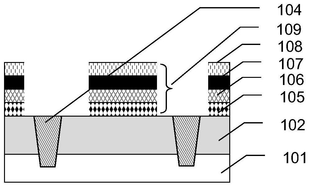
[0045] In the following specific embodiments of the present invention, please refer to figure 1 ,figure 1 It is a schematic structural diagram of a high-density phase change memory according to the first preferred embodiment of the present invention. like figure 1 As shown, a high-density phase change memory of the present invention includes, from bottom to top, Schottky diodes 105 and 106 , a phase change layer 107 and an upper electrode 108 . The Schottky diode includes a semiconductor layer 105 and a metal layer 106 that can form a Schottky barrier with the semiconductor layer 105 ; the metal layer 106 also serves as the lower electrode of the phase change layer 107 .

[0046] The high-density phase change memory of the present invention can be disposed on a semiconductor substrate 101 . The semiconductor layer 105 , the metal layer 106 , the phase change layer 107 and the upper electrode 108 are in a flat layer structure stacked from bottom to top.

[0047] In this embo...

Embodiment 2

[0054] Please refer to Figure 2-Figure 7 , Figure 2-Figure 7 is preparation figure 1 A schematic diagram of the process steps of a high-density phase change memory. like Figure 2-Figure 7 As shown, a method for preparing a high-density phase-change memory of the present invention can be used to prepare a high-density phase-change memory in the above-mentioned first embodiment, and may include the following steps:

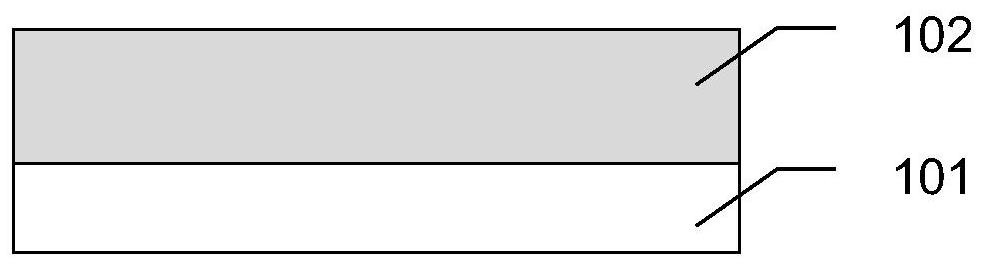
[0055] Step S01 : providing a P-type semiconductor substrate, and forming an N-type heavily doped layer on the surface of the P-type semiconductor substrate.

[0056] like figure 2 As shown, a conventional P-type Si substrate 101 can be used, and an N-type heavily doped layer 102 is formed on the surface of the P-type Si substrate 101 by ion implantation. In this embodiment, the implanted element may be As.

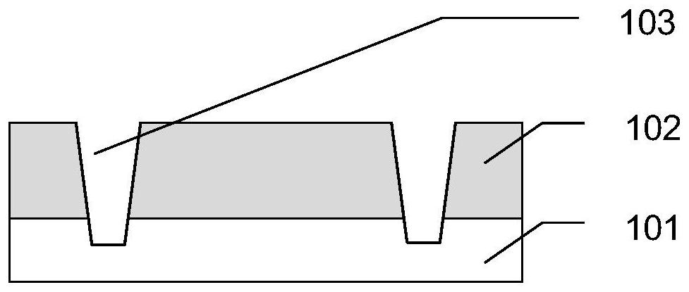
[0057] Step S02 : forming shallow trench isolation on the P-type semiconductor substrate.

[0058] like image 3 As shown, grooves 103 are formed o...

Embodiment 3

[0068] Please refer to Figure 8 , Figure 8 It is a schematic structural diagram of a high-density phase change memory according to the second preferred embodiment of the present invention. like Figure 8 As shown, a high-density phase change memory of the present invention includes, from bottom to top, Schottky diodes 205 and 208 , a phase change layer 211 and an upper electrode 212 . The Schottky diode includes a semiconductor layer 205 and a metal layer 208 that can form a Schottky barrier with the semiconductor layer. The metal layer 208 also serves as the lower electrode of the phase change layer.

[0069] Different from the first embodiment, in this embodiment, the high-density phase change memory can be arranged on a semiconductor substrate 201; The metal layer 208 is connected with a flat bottom surface and vertical sidewalls, that is, it has a cross-sectional shape such as an "L" shape; the metal layer 208 is stacked with the semiconductor layer 205 below it thro...


PUM


Abstract

The invention discloses a high-density phase-change memory, comprising from bottom to top: a Schottky diode, a phase-change layer and an upper electrode, the Schottky diode comprising a semiconductor layer and a metal layer forming a Schottky potential barrier with the semiconductor layer , the metal layer serves as the lower electrode of the phase change layer at the same time; the semiconductor layer, the metal layer, the phase change layer and the upper electrode are a flat layer structure stacked from bottom to top, or, the semiconductor layer, the phase change layer and the upper electrode are self- Bottom-up planar structure, the metal layer is connected with a planar bottom surface and vertical sidewalls, the metal layer is stacked with the semiconductor layer below it through its bottom surface, and is connected to the phase change layer above it through its sidewalls , the phase change layer is stacked with the upper electrode. The invention can effectively improve the density of the phase change memory unit, reduce the number of photolithography, simplify the process and reduce the manufacturing cost. The invention also discloses a preparation method of the above-mentioned high-density phase change memory.

Description

technical field [0001] The present invention relates to the technical field of semiconductor integrated circuit manufacturing processes, and more particularly, to a high-density phase change memory and a preparation method thereof. Background technique [0002] With the emergence of a series of new information technologies such as big data, Internet of Things, cloud computing and mobile Internet, the requirements for high read and write speed, low power consumption, high storage density, long service life and high reliability are put forward for memory. The current memory storage method is mainly DRAM+Flash. NAND Flash has high integration and low cost, but it is slow and has a short lifespan. Although DRAM is fast and has a long life, it will lose data after a power failure and cost a lot. Therefore, the development of a new type of storage technology has become a research hotspot in the industry in recent years. This type of new storage technology must have the advantages...

Claims


Application Information

Patent Timeline
Patent Type & Authority Patents(China)
IPC IPC(8): H01L27/24H01L29/47H01L29/872H01L45/00H01L21/34
CPCH01L29/47H01L29/66969H01L29/872H10B63/20H10B63/84H10N70/841H10N70/011
Inventor 钟旻陈寿面李铭
Owner SHANGHAI INTEGRATED CIRCUIT RES & DEV CENT
Why Eureka
Try Eureka