Supercharge Your Innovation With Domain-Expert AI Agents!

A kind of diode and its manufacturing method

A manufacturing method and diode technology, applied in the field of diodes, can solve problems such as poor softness of power diodes, and achieve the effect of improving softness

Active Publication Date: 2015-12-02
BYD SEMICON CO LTD
View PDF6 Cites 0 Cited by
  • Summary
  • Abstract
  • Description
  • Claims
  • Application Information

AI Technical Summary

Problems solved by technology

[0004] Aiming at problems such as poor softness of power diodes in the prior art

Method used


Image

  • A kind of diode and its manufacturing method
  • A kind of diode and its manufacturing method
  • A kind of diode and its manufacturing method

Examples


Embodiment Construction

[0026] Specific embodiments of the present invention will be described in detail below in conjunction with the accompanying drawings. It should be understood that the specific embodiments described here are only used to illustrate and explain the present invention, and are not intended to limit the present invention.

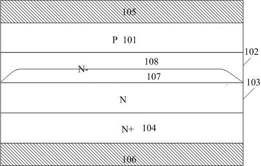
[0027] image 3 It is a schematic diagram of the structure of the diode of the present invention. It can be seen from the figure that the diode includes: N+ first semiconductor layer 104, also called substrate, under the substrate is the first metal layer 106, and the first metal layer 106 is the diode cathode. The lead-out electrode is an N-type second semiconductor layer 103 located on the N+ first semiconductor layer. The second semiconductor layer is also called an epitaxial layer. The thickness of the epitaxial layer depends on the withstand voltage required by the device. The one located on the epitaxial layer is The third semiconductor layer is also call...


PUM


Abstract

The invention relates to a semiconductor component, in particular to a diode. The diode comprises a first metal layer, a first conduction type first semiconductor layer, a first conduction type second semiconductor layer, a first conduction type third semiconductor layer, a second conduction type fourth semiconductor layer and a second metal layer, wherein the first metal layer, the first conduction type first semiconductor layer, the first conduction type second semiconductor layer, the first conduction type third semiconductor layer, the second conduction type fourth semiconductor layer and the second metal layer are connected in sequence from bottom to top. The third semiconductor layer comprises a first area and a second area, wherein the first area is arranged between the second semiconductor layer and the second area, the second area is connected with the fourth semiconductor layer arranged on the second area, and the lattice imperfection density of the first area is less than that of the second area. The diode improves the softness of the diode under the condition that power consumption of reverse recovery of the diode is not changed.

Description

technical field [0001] The invention relates to the field of semiconductors, in particular to a diode. Background technique [0002] Power Fast Recovery Diode (FRD) is a semiconductor device with good switching characteristics and short reverse recovery time. It is mainly used in electronic circuits such as switching power supplies, pulse width modulators, and frequency converters, and is widely used as high-frequency rectification, freewheeling, and damping diodes. The basic structure of a fast recovery diode is as figure 1 As shown, there is a 101P-type region connected to a metal electrode 105, 102 is an N-drift region with a low doping concentration, the drift region is located under the P-type region 101, and the N-drift region includes a first region 107 and a second region 108 , N region 103 is located under N-region 102, which is an epitaxial layer with a slightly higher doping concentration than 102, N+104 is located under N region 103, which is a high-concentrati...

Claims


Application Information

Patent Timeline
Patent Type & Authority Patents(China)
IPC IPC(8): H01L29/861H01L29/32H01L21/322H01L21/329
CPCY02P70/605Y02P70/50
Inventor 肖秀光黄定园吴海平
Owner BYD SEMICON CO LTD
Features
  • R&D
  • Intellectual Property
  • Life Sciences
  • Materials
  • Tech Scout
  • Unparalleled Data Quality
  • Higher Quality Content
  • 60% Fewer Hallucinations
Learn More