Structure of semiconductor and manufacture process of semiconductor

A manufacturing process and semiconductor technology, applied in the fields of semiconductor/solid-state device manufacturing, semiconductor devices, electrical components, etc., can solve the problems of electrical instability of the gate structure, deterioration of the NBTI value, and complex control of the integrated technology manufacturing process, and achieve improvement. Equivalent work function value, the effect of increasing electrical stability

Active Publication Date: 2013-05-22
UNITED MICROELECTRONICS CORP
View PDF6 Cites 2 Cited by
  • Summary
  • Abstract
  • Description
  • Claims
  • Application Information

AI Technical Summary

Problems solved by technology

[0003] However, with the rapid shrinkage of semiconductor technology to the nanometer level, even the work function (work function) metal gate structure will reach its physical and electrical limitations, which may lead to electrical instability of the gate structure, NBTI ( negative bias temperature instability) value degradation and other issues
Even, taking complementary metal-oxide semiconductor (CMOS) technology as an example, since its dual work function metal gate needs to be matched with NMOS devices and PMOS devices, it makes the integration of related components Technology and manufacturing process control are more complicated and the manufacturing process effect that can be achieved is limited. Therefore, how to improve the electrical quality of the gate structure of PMOS devices or NMOS devices, such as increasing their work function value, is an urgent and urgent need today. major issues of concern

Method used


Image

  • Structure of semiconductor and manufacture process of semiconductor
  • Structure of semiconductor and manufacture process of semiconductor
  • Structure of semiconductor and manufacture process of semiconductor

Examples


Embodiment Construction

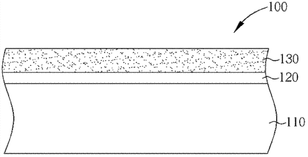
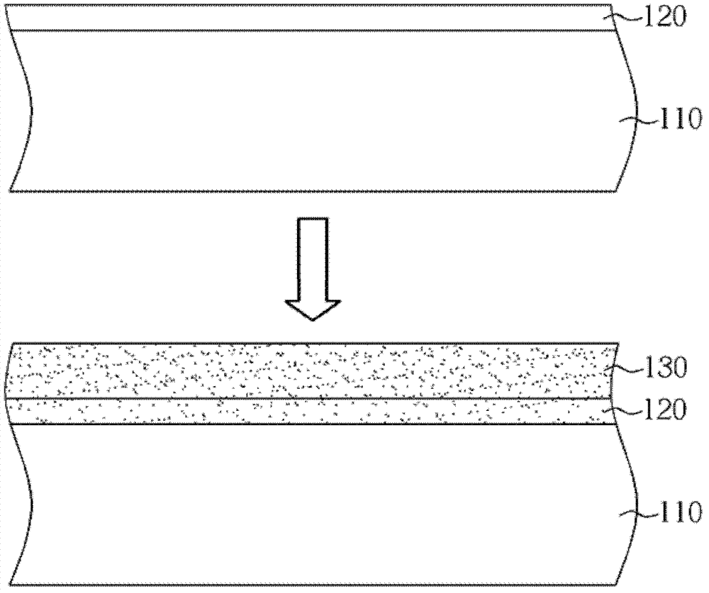
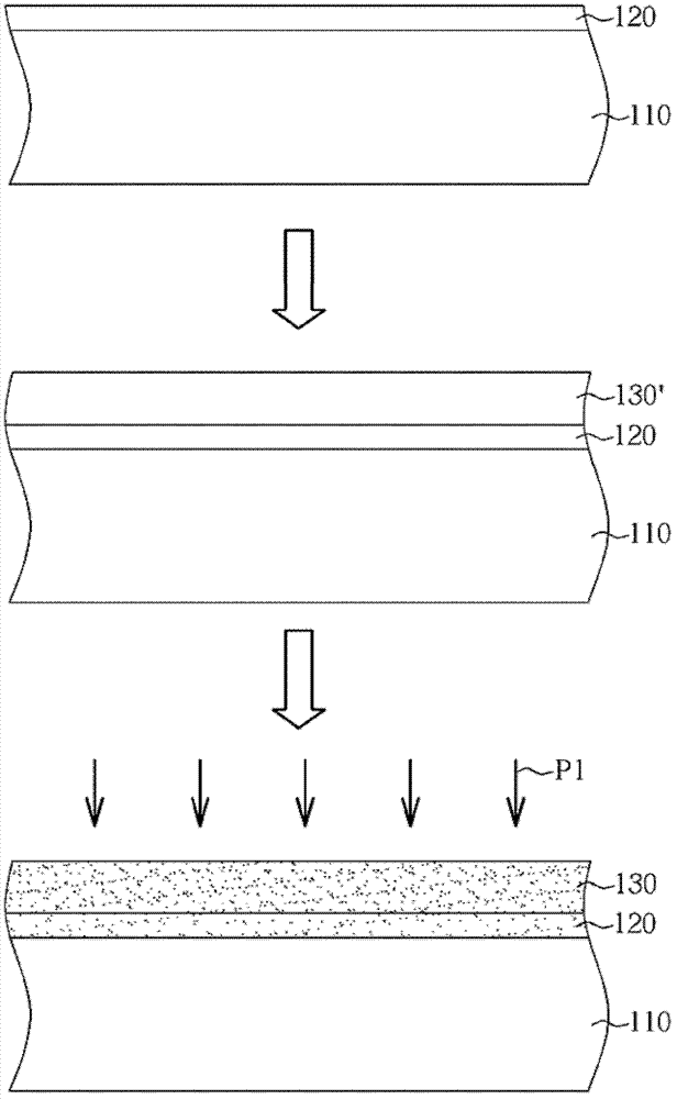
[0031] figure 1 A schematic cross-sectional view of a semiconductor structure according to an embodiment of the present invention is shown. Such as figure 1 As shown, the semiconductor structure 100 includes a substrate 110 , a dielectric layer 120 and a fluorine-containing metal layer 130 . The dielectric layer 120 is on the substrate 110 . The metal layer 130 containing fluorine is located on the dielectric layer 120 . The substrate 110 includes a silicon substrate, a silicon-containing substrate, a III-V silicon-on-silicon substrate (such as GaN-on-silicon), a graphene-on-silicon substrate (graphene-on-silicon), or a silicon-on-insulator substrate. , SOI) substrates and other semiconductor substrates. The dielectric layer 120 includes a high-k dielectric layer, such as a metal-containing dielectric layer, which may include hafnium oxide and zirconium oxide, but the invention is not limited thereto. Furthermore, the high-k dielectric layer can be selected from hafnium o...


PUM


Abstract

The invention discloses a structure of a semiconductor and a manufacture process of the semiconductor. The structure of the semiconductor comprises a substrate, a dielectric layer and a metal layer with fluorine contained, wherein the dielectric layer is located on the substrate, and the metal layer with the fluorine contained is located on the dielectric layer. In addition, further disclosed is the manufacture process of the semiconductor, and the manufacture process is capable of forming the structure of the semiconductor.

Description

technical field [0001] The invention relates to a semiconductor structure and its manufacturing process, in particular to a semiconductor structure with a fluorine-containing metal layer and its manufacturing process. Background technique [0002] In the existing semiconductor industry, polysilicon is widely used in semiconductor devices such as metal-oxide-semiconductor (MOS) transistors as a standard gate filling material. However, as the size of MOS transistors continues to shrink, the performance of traditional polysilicon gates is reduced due to the boron penetration effect, and the unavoidable depletion effect and other problems make the equivalent gate dielectric The thickness of the electrical layer increases and the capacitance of the gate decreases, which in turn leads to the decline of the driving ability of the device and other difficulties. Therefore, the semiconductor industry is trying to use new gate filling materials, such as using work function metals to r...

Claims


Application Information

Patent Timeline
Patent Type & Authority Applications(China)
IPC IPC(8): H01L29/423H01L21/285
Inventor 林坤贤林俊贤黄信富
Owner UNITED MICROELECTRONICS CORP
Why Eureka
Try Eureka