Step printed circuit board and manufacture method of the step printed circuit board

A printed circuit board and manufacturing method technology, applied in the directions of printed circuit manufacturing, printed circuit, multilayer circuit manufacturing, etc., can solve the problems of stepped groove deformation, pressing warpage, difficult stepped board processing, etc.

Active Publication Date: 2013-05-29
NEW FOUNDER HLDG DEV LLC +1
View PDF3 Cites 32 Cited by
  • Summary
  • Abstract
  • Description
  • Claims
  • Application Information

AI Technical Summary

Problems solved by technology

However, the method of filling with cushioning materials such as silica gel may cause defects such as insufficient matching between the silica gel and the stepped groove, gaps or misalignment, resulting in deformation of the stepped groove after lamination, warping of the pressing, excessive glue overflow or insufficient flow of glue in the groove, etc.
At the same time, there are certain limitations in the size and shape of the stepped groove, and it is difficult to realize the processing of the stepped plate with via holes in the stepped groove area

Method used


Image

  • Step printed circuit board and manufacture method of the step printed circuit board
  • Step printed circuit board and manufacture method of the step printed circuit board
  • Step printed circuit board and manufacture method of the step printed circuit board

Examples


Embodiment Construction

[0018] The embodiments of the present invention will be further described in detail below in conjunction with the accompanying drawings.

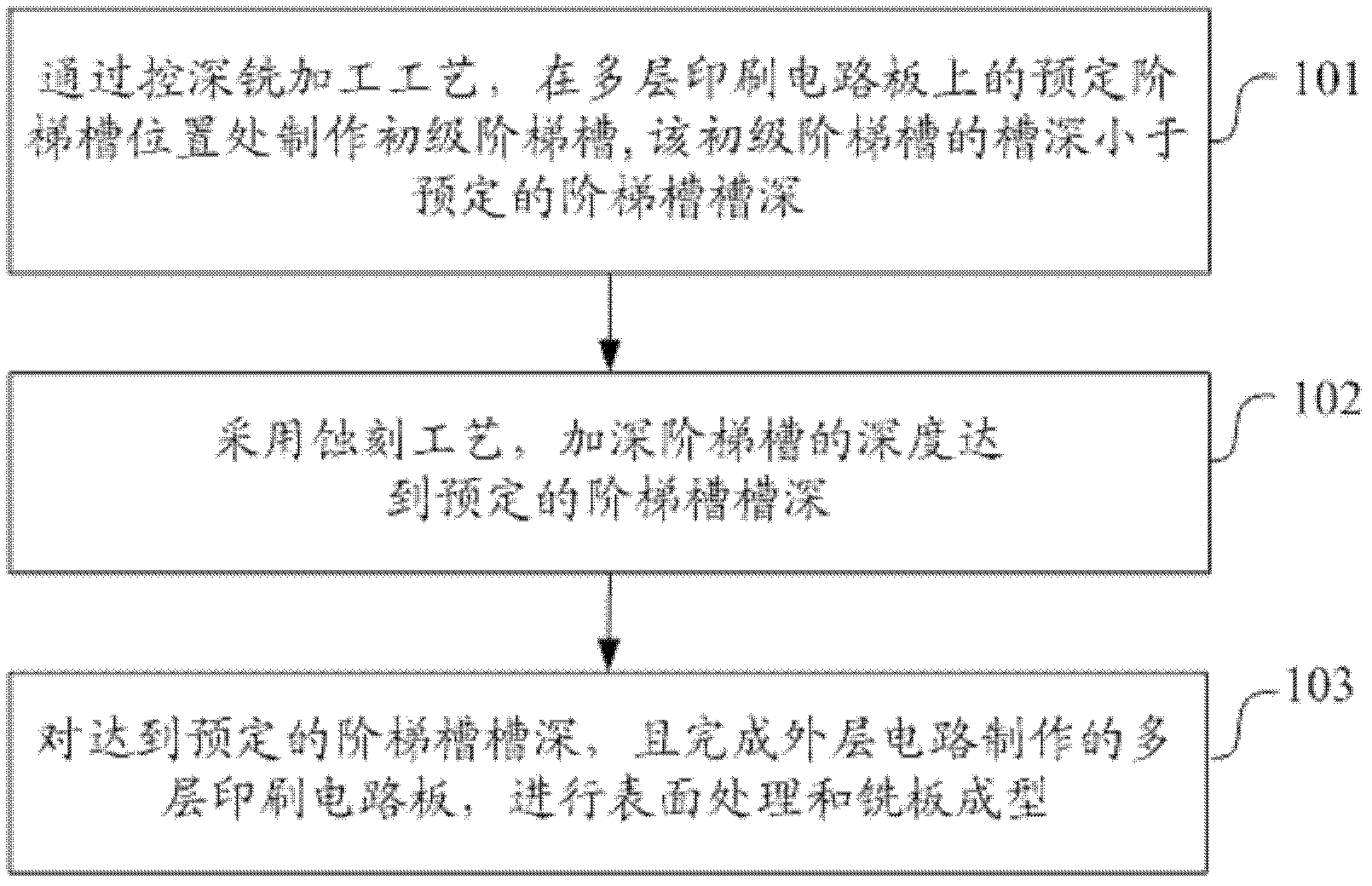
[0019] An embodiment of the present invention provides a method for manufacturing a stepped printed circuit board, such as figure 1 shown, including the following steps:

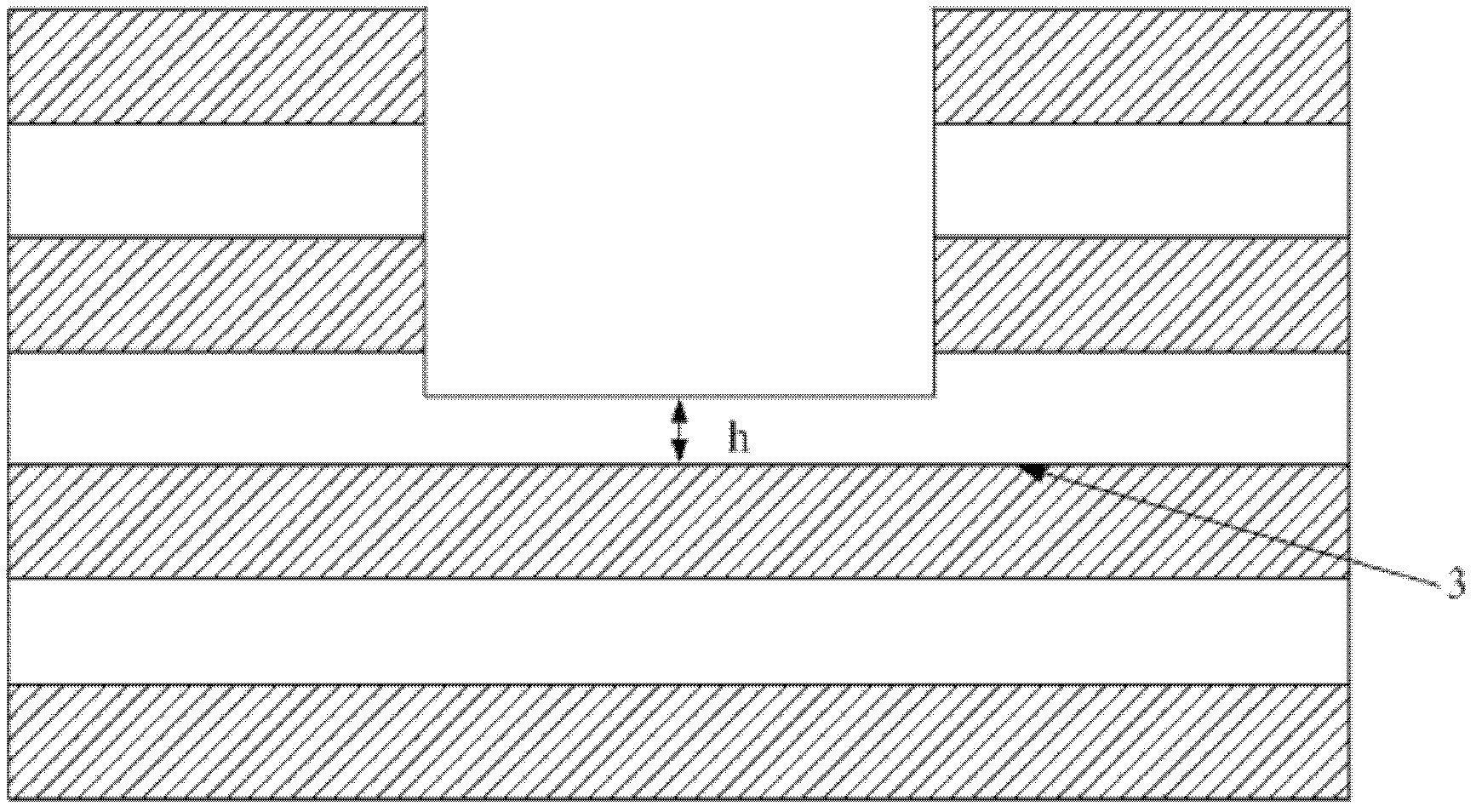
[0020] Step 101, through the depth-controlled milling process, make a primary stepped groove at the predetermined stepped groove position on the multilayer printed circuit board, and the groove depth of the primary stepped groove is smaller than the predetermined stepped groove depth;

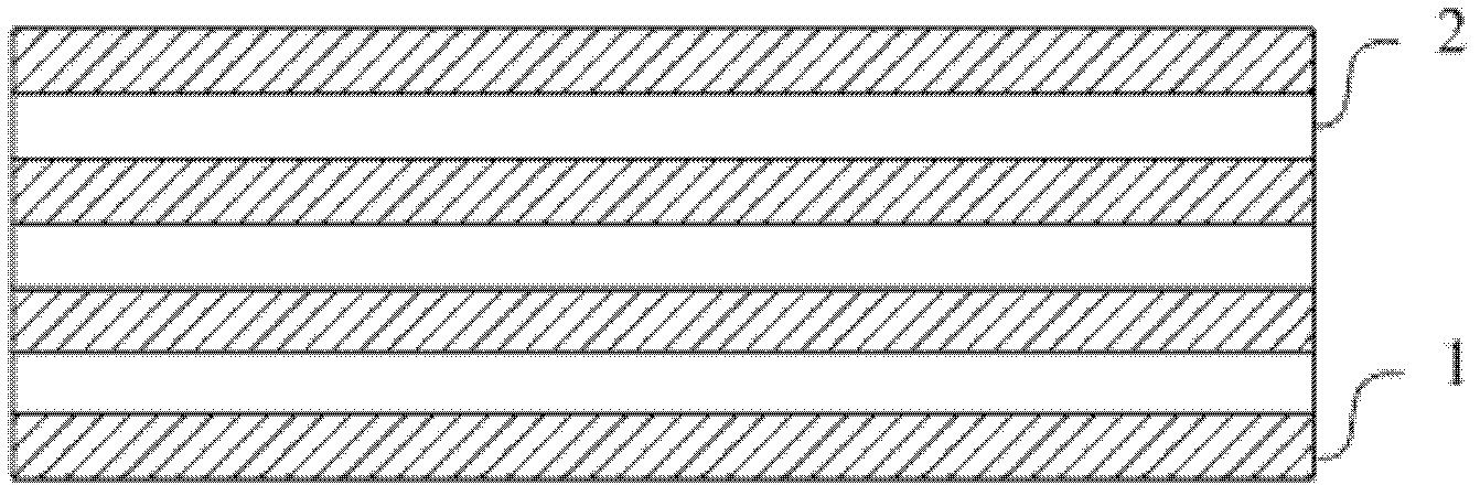
[0021] Specifically, when manufacturing a stepped printed circuit board, it is necessary to firstly manufacture a plurality of printed circuit boards to be laminated; to laminate a plurality of printed circuit boards to form a multilayer printed circuit board. Moreover, after copper plating is performed on the surface of the multilayer printed circuit board, the outer layer circuit is mad...


PUM


Abstract

The invention belongs to the technical field of printed circuit board and in particular to a step printed circuit board and a manufacture method of the step printed circuit board. Deep milling processing technology is controlled, step grooves are roughly manufactured at preset step groove positions on a multilayer printed circuit board manufactured by an outer layer circuit, and then the roughly manufactured step grooves are further exacted to a preset depth through etching technology. The step printed circuit board and the manufacture method of the step printed circuit board have the advantages of being simple in process, easy to control, high in processing reliability and wide in application range, step groove lateral walls manufactured by the method are flat and little in defects, and accordingly high yield can be ensured. Simultaneously, the method does not need to consume auxiliary materials, and manufactured cost is saved.

Description

technical field [0001] The invention relates to the technical field of printed circuit boards, in particular to a stepped printed circuit board and a manufacturing method thereof. Background technique [0002] The stepped printed circuit board in the prior art refers to a multilayer printed circuit board with stepped grooves. Multilayer printed circuit boards include conventional stepped printed circuit boards and special stepped printed circuit boards. At present, when making special stepped printed circuit boards, low-flow prepreg (low-flow PP) is often used to open windows, and after lamination, step grooves are made by controlled depth milling or laser cutting. However, the use of low-flow PP is likely to cause local voids or slot deformation in the adhesive layer due to insufficient and uneven glue flow during the lamination process. [0003] In the prior art, the cushioning properties of "aluminum sheet + silica gel sheet" are used to distribute the flow glue evenly,...

Claims


Application Information

Patent Timeline
Patent Type & Authority Applications(China)
IPC IPC(8): H05K3/00H05K3/46
Inventor 康益平罗龙金轶蔡童军宣光华
Owner NEW FOUNDER HLDG DEV LLC
Why Eureka
Try Eureka