
Loop circuit compensating circuit

A loop compensation and circuit technology, applied in the direction of adjusting electrical variables, control/regulating systems, instruments, etc., can solve the problems of large layout area, excessive circuit layout, unfavorable product miniaturization, etc., to reduce the layout area, The effect of increasing power consumption

Active Publication Date: 2013-06-05
SHANGHAI HUAHONG GRACE SEMICON MFG CORP
View PDF5 Cites 5 Cited by
  • Summary
  • Abstract
  • Description
  • Claims
  • Application Information

AI Technical Summary

Problems solved by technology

The compensation circuit needs to use capacitors, and the capacitors used in traditional circuits need to occupy a relatively large layout area, resulting in an excessively large circuit layout that is not conducive to product miniaturization

Method used


Image

  • Loop circuit compensating circuit
  • Loop circuit compensating circuit

Examples


Embodiment Construction

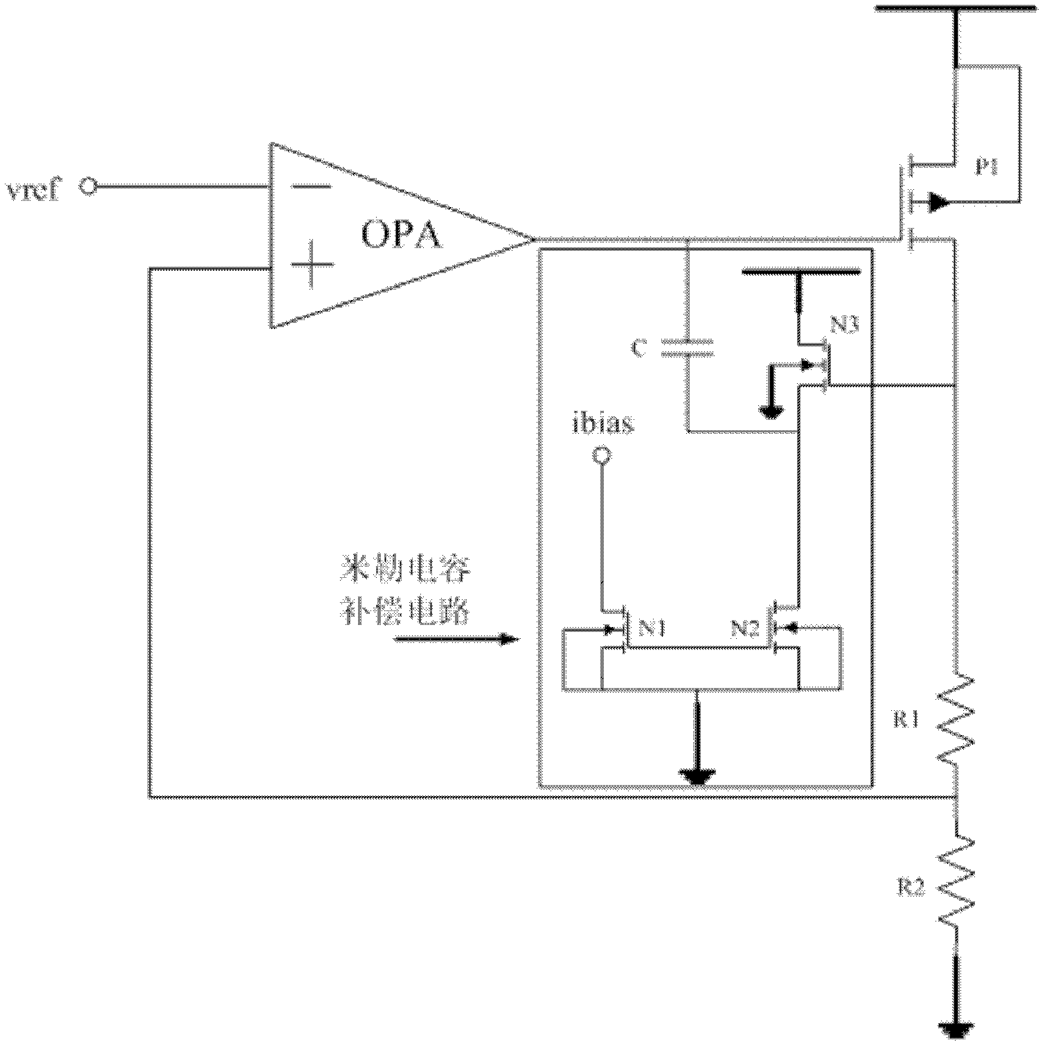
[0023] like figure 2 As shown, the loop compensation circuit of the present invention includes: an operational amplifier OPA, its negative input terminal is connected to the reference voltage, its positive input terminal is grounded through a resistor R2, and its output terminal is connected to the gate of the PMOS transistor P1;

[0024] PMOS transistor P1, its source is connected to the power supply, and its drain is grounded through resistor R1 and resistor R2;

[0025] Capacitor C, its positive terminal is connected to the gate of PMOS transistor P1, and its negative terminal is connected to the source of NMOS transistor N3;

[0026] NMOS transistor N3, its gate is connected to the drain of PMOS transistor P1, its drain is connected to the power supply, and its source is connected to the drain of NMOS transistor N2;

[0027] The source of the NMOS transistor N1 is connected to the source of the NMOS transistor N2 and then grounded, which is connected to the gate of the N...


PUM


Abstract

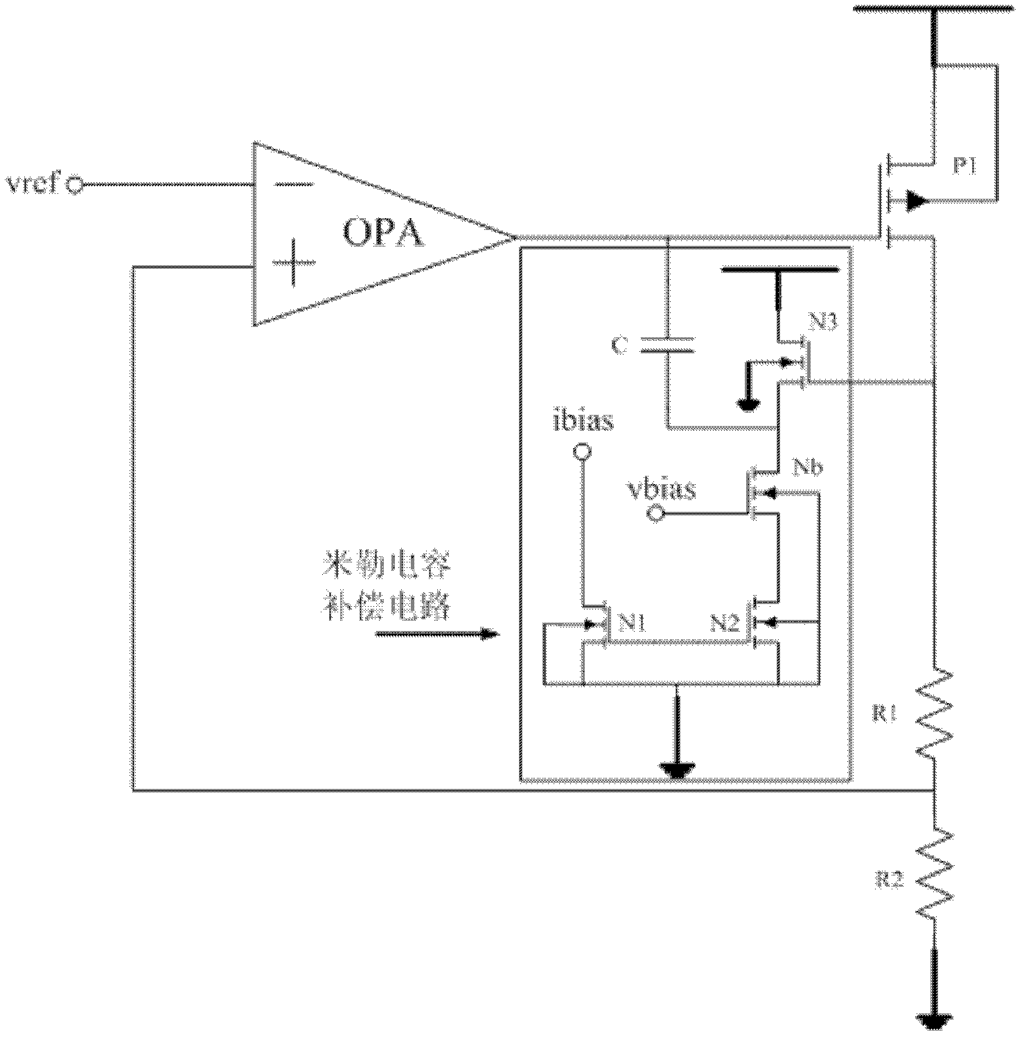
The invention discloses a loop circuit compensating circuit which comprises an operational amplifier (OPA), a p-channel metal oxide semiconductor (PMOS) pipe (P1), a capacitor (C), an n-channel metal oxide semiconductor (NMOS) pipe (N3), and an n-channel metal oxide semiconductor (NMOS) pipe (N1), wherein the negative input end of the OPA is connected with a reference voltage, the positive input end of the OPA is connected to the ground through a resistor R2, the output end of the OPA is connected with a grid electrode of the PMOS pipe (P1), a source electrode of the PMOS pipe (P1) is connected with a power source, a drain electrode of the PMOS pipe (P1) is connected to the ground through a resistor R1 and the resistor R2, the positive end of the C is connected with the grid electrode of the PMOS pipe (P1), the negative end of the C is connected with a source electrode of a NMOS pipe (N2), a source electrode of the NMOS pipe (N1) is connected with a source electrode of the NMOS pipe (N2) and then is connected to the ground, the source electrode of the NMOS pipe (N1) is connected with a grid electrode of the NMOS pipe (N2), a drain electrode of the NMOS pipe (N1) is connected with a configuration input bias current (IBIAS), substrates of the NMOS pipe (N1), the NMOS pipe (N2) and the NMOS pipe (N3) are connected with to the ground. The source electrode of the NMOS pipe (N3) is connected with the drain electrode of the NMOS pipe (N2) through a NMOS pipe (Nb), an drain electrode of the NMOS pipe (Nb) is connected with source electrode of the NMOS pipe (N3), a source electrode of the NMOS pipe (Nb) is connected with the drain electrode of the NMOS pipe (N2), and an grid electrode of the NMOS pipe (Nb) is connected with a bias voltage (VBIA), and a substrate of the NMOS pipe (Nb) is connected to the ground. The loop circuit compensating circuit can reduce a capacitance valve and a layout area on the premise that additional power consumption does not increased, and the fact that a phase margin and a gain margin are not changed is guaranteed.

Description

technical field [0001] The invention relates to the field of integrated circuits, in particular to a loop compensation circuit. Background technique [0002] In the CTAT (Conversional to Absolute Temperature) current generation circuit, in order to ensure the stable operation of the circuit, it is necessary to compensate the Miller capacitance of the feedback loop to meet a certain phase margin and gain margin. The compensation circuit needs to use capacitors, and the capacitors used in traditional circuits need to occupy a relatively large layout area, resulting in an excessively large circuit layout that is not conducive to product miniaturization. Contents of the invention [0003] The technical problem to be solved by the present invention is to provide a loop compensation circuit, which can reduce the capacitance value and layout area without increasing the extra power consumption and keeping the phase margin and gain margin unchanged. [0004] In order to solve the ...

Claims


Application Information

Patent Timeline
Patent Type & Authority Applications(China)
IPC IPC(8): G05F1/10
Inventor 袁志勇
Owner SHANGHAI HUAHONG GRACE SEMICON MFG CORP
Learn More