Semiconductor device and method for fabricating the same

A device manufacturing method and semiconductor technology, applied in the direction of semiconductor/solid-state device manufacturing, semiconductor devices, semiconductor/solid-state device components, etc., can solve problems such as electrical failures, and achieve the effect of preventing outflow or dispersion

Inactive Publication Date: 2013-06-05
SOCIONEXT INC
View PDF6 Cites 5 Cited by
  • Summary
  • Abstract
  • Description
  • Claims
  • Application Information

AI Technical Summary

Problems solved by technology

This can cause electrical failure

Method used


Image

  • Semiconductor device and method for fabricating the same
  • Semiconductor device and method for fabricating the same
  • Semiconductor device and method for fabricating the same

Examples


Embodiment Construction

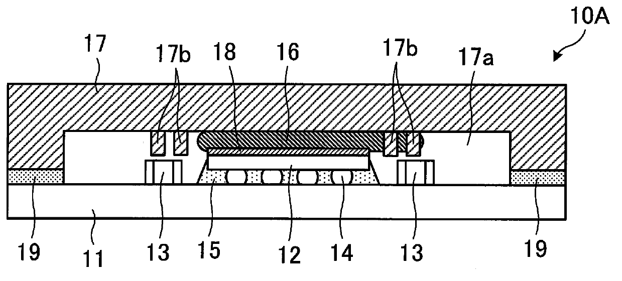
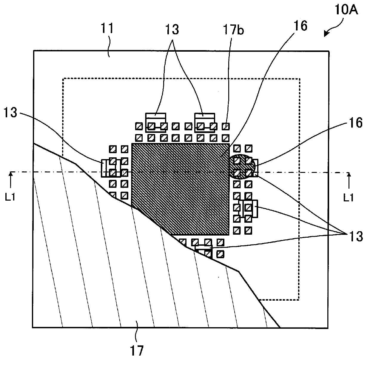
[0047] First, the first embodiment will be described. Figure 1A and Figure 1B is an example of the semiconductor device according to the first embodiment. Figure 1B is a schematic plan view of an example of the semiconductor device according to the first embodiment. Figure 1A is along Figure 1B Schematic cross-sectional view of the line L1-L1.

[0048] A semiconductor device 10A according to the first embodiment includes a substrate (wiring substrate) 11 and a semiconductor element (semiconductor chip) 12 and a plurality of electronic components 13 mounted on the substrate 11 .

[0049] Each of the substrate 11 and the semiconductor element 12 has electrode pads ( Figure 1A or Figure 1B not shown). The electrode pads of the substrate 11 are electrically connected to a plurality of conductive parts (not shown), such as a plurality of wires or a plurality of via holes formed in the substrate 11 . Electrode pads of the semiconductor element 12 are connected to electrod...


PUM


Abstract

A semiconductor device includes a semiconductor element placed over a substrate, a heat conducting material placed over the semiconductor element, and a radiator placed over the heat conducting material. The radiator has a plurality of projections which are arranged outside a region opposite to the semiconductor element and which protrude toward the substrate. Even if the heat conducting material flows out from over the semiconductor element at fabrication time, the heat conducting material which flows out is made by the plurality of projections to adhere to and spread along the radiator. As a result, the outflow or scattering of the heat conducting material toward the substrate or an electric trouble caused by it is prevented.

Description

technical field [0001] Embodiments discussed herein relate to a semiconductor device and methods of manufacturing the same. Background technique [0002] A technique of connecting a heat sink such as a heat sink or a heat sink to a semiconductor element included in a semiconductor device via a thermally conductive material such as solder or bonding agent and emitting heat generated by the semiconductor element by using the heat sink is well known. [0003] For example, such a semiconductor device assembly method is as follows. Heat is applied to a thermally conductive material (such as solder) placed between a semiconductor element and a heat sink to melt it and then solidify it. The semiconductor element and the heat sink are bonded with a thermally conductive material such as bonding compound. [0004] For a semiconductor device assembled in this way, for example, a technique of fixing a frame-shaped partition surrounding a semiconductor element on a heat sink and accomm...

Claims


Application Information

Patent Timeline
Patent Type & Authority Applications(China)
IPC IPC(8): H01L23/367H01L21/50
CPCH01L2924/19105H01L2924/16251H01L21/50H01L2224/73204H01L2224/32245H01L2224/73253H01L23/367H01L23/42H01L23/3675H01L2224/8314H01L2224/26165H01L2224/16225H01L2224/26175H01L2224/32225H01L2924/00
Inventor 井原匠
Owner SOCIONEXT INC
Why Eureka
Try Eureka