PXIe interface Nand Flash data steam disc access accelerating method

A data flow and data loading technology, applied in the direction of input/output to record carrier, etc., can solve the mismatch of NandFlash access rate PXIExpress high-speed interface rate, can not maximize the NandFlash array access speed, I/O rate requirements are very high Advanced problems, to achieve the effect of saving logic resources, reducing requirements, and high access speed

Active Publication Date: 2013-06-12
HARBIN INST OF TECH
View PDF6 Cites 5 Cited by
  • Summary
  • Abstract
  • Description
  • Claims
  • Application Information

AI Technical Summary

Problems solved by technology

[0008] In order to solve the problem that the high-speed data flow disk has high requirements on the I / O rate, the access speed of the Nand Flash array cannot be improved to the maximum extent, and the Nand Flash access rate does not match the PXI Express high-speed interface rate, the present invention proposes the PXIe interface Nand Flash data stream disk access acceleration method

Method used


Image

  • PXIe interface Nand Flash data steam disc access accelerating method
  • PXIe interface Nand Flash data steam disc access accelerating method
  • PXIe interface Nand Flash data steam disc access accelerating method

Examples


specific Embodiment approach 1

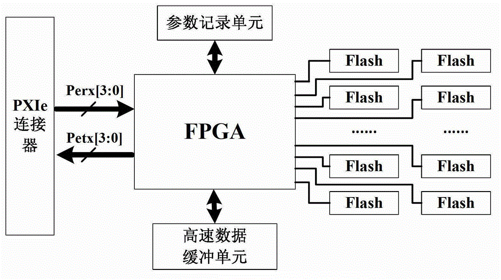
[0022] Specific implementation mode 1. Combination figure 1 Describe this embodiment in detail, the PXIe interface Nand Flash data streaming disk access acceleration method described in this embodiment is based on 4 Nand Flash chips connected in parallel to form 4 minimum control units, and the control lines of each Nand Flash chip are shared , I / O lines are connected in parallel, and each Nand Flash chip includes registers and storage arrays inside the Nand Flash chip, and the method comprises the following steps:

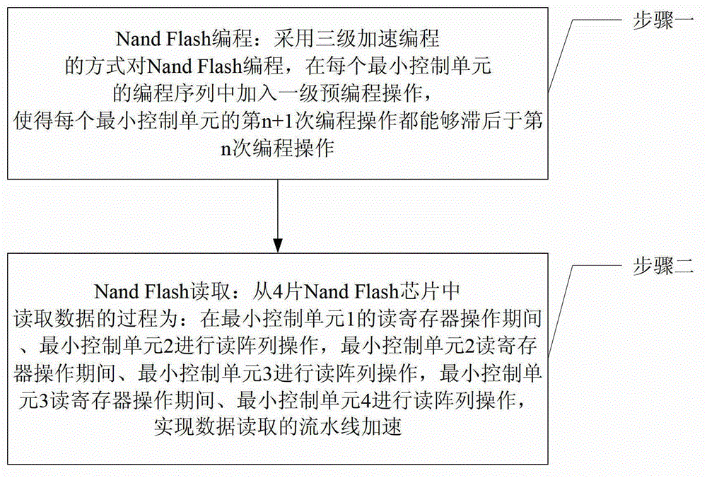
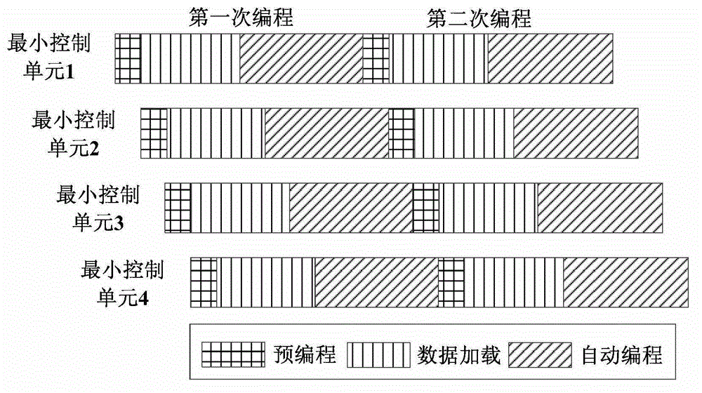
[0023] Step 1. Nand Flash programming: Program Nand Flash using three-level accelerated programming, and add a level of pre-programming operation to the programming sequence of each minimum control unit, so that the n+1th programming operation of each minimum control unit are capable of lagging behind the nth programming operation, such as image 3 as shown,

[0024] Wherein, n is an integer; said pre-programming is short-time programming,

[0025] Step 2, Nan...

specific Embodiment approach 2

[0035] Embodiment two, the difference between this embodiment and the PXIe interface Nand Flash data stream disk access acceleration method described in Embodiment one is that each piece of Nand Flash programming described in step one includes two processes of data loading and automatic programming ,

[0036] Data loading is to write data from the external Nand Flash controller to the internal register of the Nand Flash chip, the typical time is 204.8μs;,;

[0037] Automatic programming is the programming of data from the internal registers of the Nand Flash chip to the storage array. During the automatic programming process, the typical time is 300μs. During the automatic programming process, the Nand Flash chip cannot be loaded with data.

specific Embodiment approach 3

[0038] Specific embodiment three, the difference between this embodiment and the PXIe interface Nand Flash data stream disk access acceleration method described in specific embodiment one is that the Nand Flash described in step two reads and includes two read array operations and read register operations process,

[0039] The read array operation is to read the data in the Nand Flash storage array into the internal register of the Nand Flash chip, the typical time is 50μs, and other operations on the Nand Flash chip cannot be performed during the read array process;

[0040] The read register operation is to read data from the internal register of the Nand Flash chip to the outside of the chip, and the typical time is 254.8μs, such as Figure 7 shown.

[0041] Since the programming data all come from the high-speed data buffer, the programming data must be read out in order before the data loading operation can be performed on each minimum control unit in turn. The sum of ...


PUM


Abstract

The invention relates to a PXIe interface Nand Flash data steam disc access accelerating method, aiming at solving the problems that a high-speed data stream disc has a very high requirement on I/O (Input/Output) speed, the access speed of Nand Flash arrays cannot be improved to the utmost extent, and the Nand Flash access speed is not matched with the PXI (PCI Extensions for Instrumentation) Express high-speed interface speed. The method comprises the steps of adopting a three-level acceleration programming method to program Nand Flash, and adding first-level preprogramming operation in the programming sequence of each minimum control unit to enable the n+1 programming operation of each minimum control unit to lag behind the n programming operation of each minimum control unit; and reading data from four Nand Flash chips to realize the streamline acceleration of data reading. The PXIe interface Nand Flash data steam disc access accelerating method is applicable to the field of testing.

Description

technical field [0001] The invention relates to a data stream disk access acceleration method, in particular to a PXIe interface Nand Flash data stream disk access acceleration method. Background technique [0002] In the field of testing, a large number of applications for mass data storage and recording have emerged, including military reconnaissance, satellite communications, video testing, spectrum monitoring, continuous waveform generation, collision testing and other testing applications that require long-term streaming of massive data. The raw data to be collected is stored in real time for later analysis. [0003] In the past, data streaming to disk was generally completed by traditional desktop instruments or dedicated custom hardware. For desktop instruments, the onboard storage capacity is limited, and the analysis results of the original data are often sent back to the computer after the data collection is completed. If the original test data is to be transmitte...

Claims


Application Information

Patent Timeline
Patent Type & Authority Applications(China)
IPC IPC(8): G06F3/06
Inventor 刘兆庆乔立岩黄敏朱雨杜威达彭喜元
Owner HARBIN INST OF TECH
Why Eureka
Try Eureka