
Photosensing unit and manufacturing method thereof

A light-sensing element and manufacturing method technology, which is applied in the manufacture of electrical components, semiconductor devices, and final products, and can solve problems such as the inability to present a linear relationship between photocurrent and light illuminance

Active Publication Date: 2013-06-12
AU OPTRONICS CORP
View PDF2 Cites 2 Cited by
  • Summary
  • Abstract
  • Description
  • Claims
  • Application Information

AI Technical Summary

Problems solved by technology

[0006] In order to overcome the defects of the prior art, the object of the present invention is to provide a light sensing element, so as to improve the problem that the photocurrent and the light illuminance cannot show a linear relationship

Method used


Image

  • Photosensing unit and manufacturing method thereof
  • Photosensing unit and manufacturing method thereof
  • Photosensing unit and manufacturing method thereof

Examples


Embodiment Construction

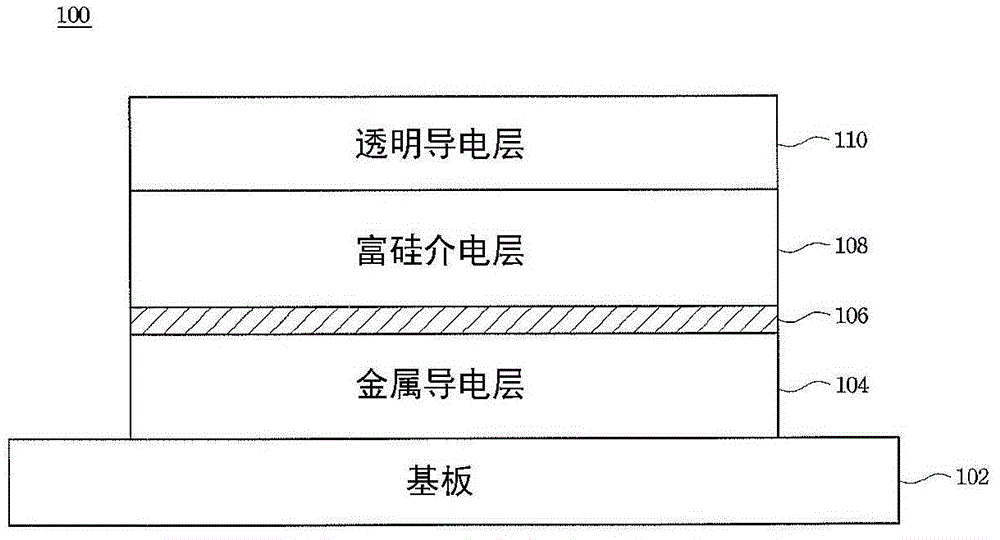
[0026] figure 1 According to an embodiment of the present invention, a schematic cross-sectional view of a photo-sensing element is shown. Such as figure 1 As shown, the partially enlarged part of the light sensing element 100 (such as: ambient light sensor, ALS) includes a substrate 102, a metal conductive layer (or conductive layer) 104, an interface dielectric layer 106, a silicon-rich The dielectric layer 108 and a transparent conductive layer 110 . Among them, the metal conductive layer 104 is formed on the substrate 102, the interfacial dielectric layer 106 is formed on the metal conductive layer 104, the silicon-rich dielectric layer 108 is formed on the interfacial dielectric layer 106, and the transparent conductive layer 110 is formed on the rich on the silicon dielectric layer 108 . The metal conductive layer 104 , the interface dielectric layer 106 , the silicon-rich dielectric layer 108 and the transparent conductive layer 110 in the light sensing element 100 c...


PUM

PropertyMeasurementUnit
thicknessaaaaaaaaaa
thicknessaaaaaaaaaa
thicknessaaaaaaaaaa

Abstract

The invention relates to a photosensing unit, which comprises a metal conductive layer, an interface dielectric layer, a silicon-rich dielectric layer and a transparent conductive layer, wherein the interface dielectric layer is formed on the metal conductive layer; the silicon-rich dielectric layer is formed on the interface dielectric layer; and the transparent conductive layer is formed on the silicon-rich dielectric layer. The problem that light current and light illuminance cannot have a linear relation can be improved so as to improve the quality of the photosensing unit.

Description

[0001] This application is a divisional application of the invention patent application with the application number 200810170472.6, the application date is November 06, 2008, and the invention title is "light sensing element and its manufacturing method". technical field [0002] The present invention relates to a light sensing element, and in particular to an ambient light sensor (Ambient Light Sensor, ALS). Background technique [0003] In the known technology, when fabricating the ambient light sensor (Ambient Light Sensor, ALS) on the TFT-LCD display panel, because the amorphous silicon (α-Si) or polycrystalline silicon (poly-Si) thin film is sensitive to visible light (400 nanometers ~ 700 nanometers) and near-infrared light (700 nanometers to 1.1 microns) have strong sensitivity, so amorphous silicon or polysilicon thin films are usually used as the basic material for making ambient light sensors, but due to The photosensitivity of amorphous silicon or polysilicon thin...

Claims


Application Information

Patent Timeline
Patent Type & Authority Applications(China)
IPC IPC(8): H01L31/08H01L31/02H01L31/18
CPCY02P70/50
Inventor 陈信学刘婉懿彭佳添许宗义曾任培
Owner AU OPTRONICS CORP
Learn More