

Clamp-like movement delayed circuit with output signal repeat sycle different from input signal
An input signal, delay circuit technology, applied in the direction of single output arrangement, automatic power control, generation/distribution of signals, etc., can solve the problem of not considering the layout of delay lines, etc.
- Summary
- Abstract
- Description
- Claims
- Application Information
AI Technical Summary
Problems solved by technology
Method used
Image

Examples
Embodiment Construction
[0025] specific implementation plan
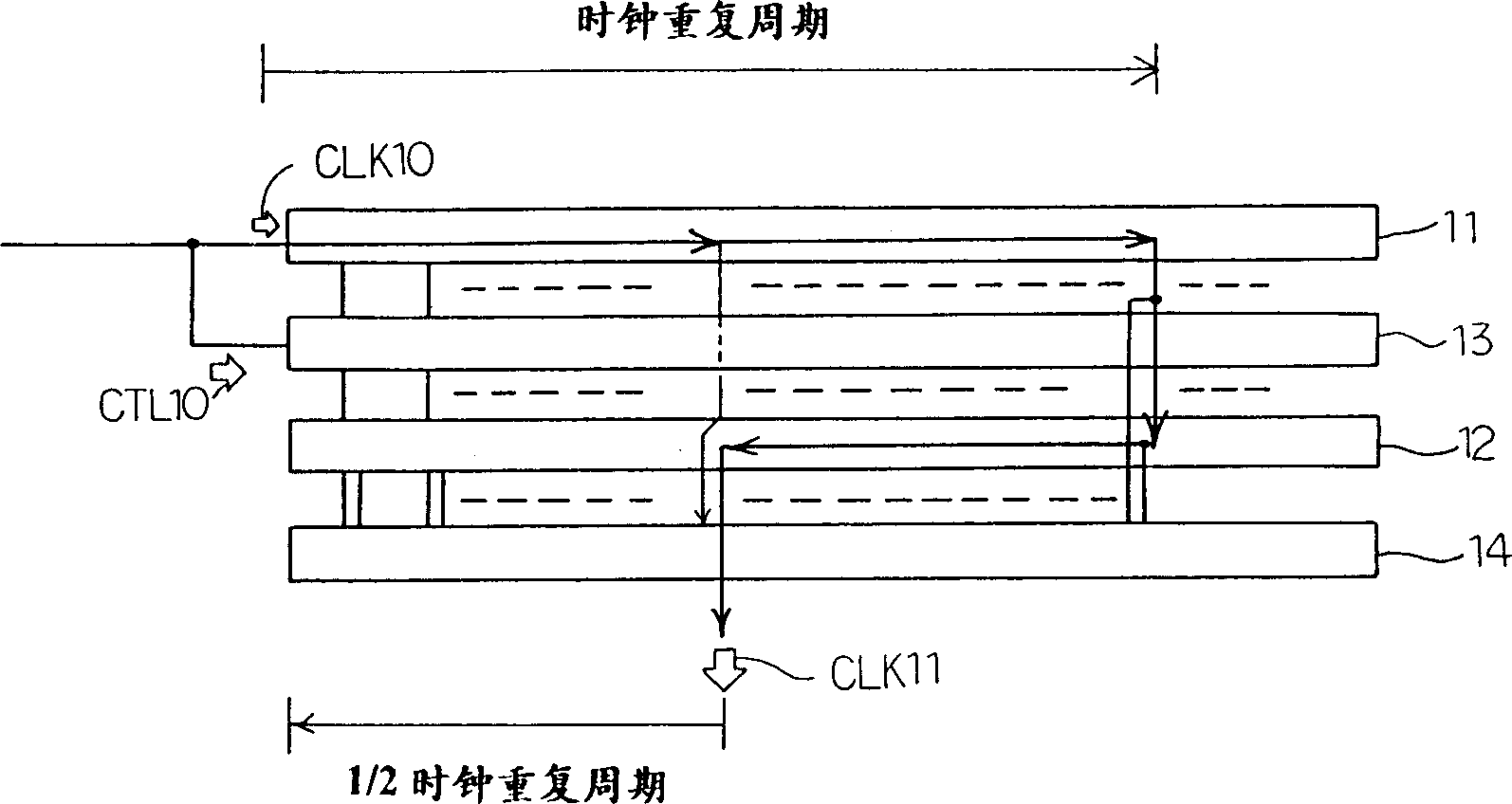
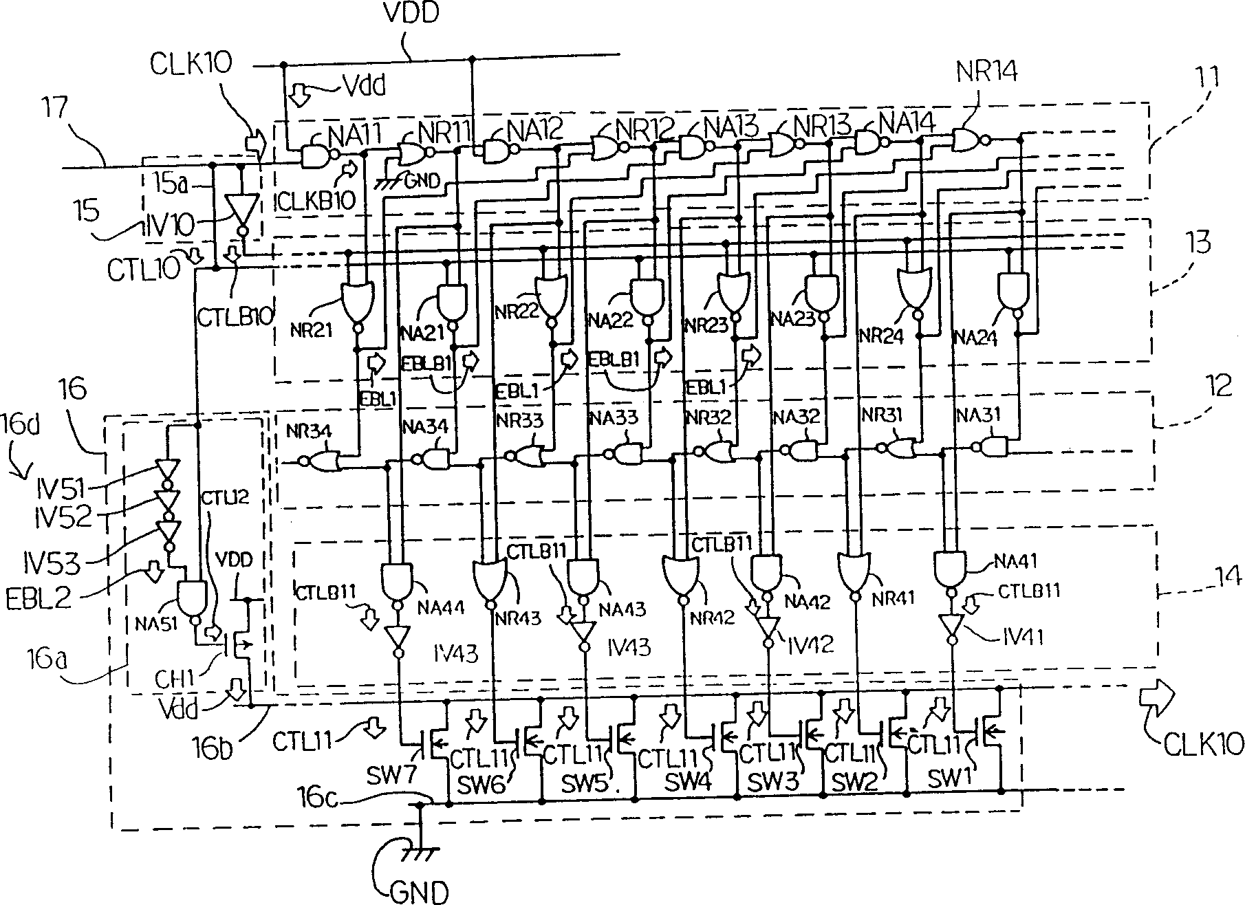
[0026] see first figure 2 , embodies the delay circuit of the present invention by a first delay line 11 that transmits the input clock signal CLK10 to the right, a second delay line 12 that transmits the clock signal CLK10 to the left, and a second delay line 12 that is connected to the first delay line 11 and the second delay line 12 A transfer circuit 13 for transferring a group of clock signals CLK10 from the first delay line 11 to the second delay line 12, and a transfer circuit 13 connected between the first delay line 11 and the second delay line 12 to generate the output clock signal Comparator 14 of CLK11 constitutes. The transfer circuit 13 is responsive to the next clock signal CLK10 serving as the timing control signal CTL10 , and transfers a set of clock signals CLK10 from the first delay line 11 to the second delay line 12 . The direction in which the second delay line 12 transmits the clock signal CLK10 is opposite to tha...
PUM
 Abstract
Description
Claims
Application Information