Manufacturing Technology of In-mold Injection Molding Circuit

An inlay injection molding and manufacturing process technology, applied in the direction of coating, etc., can solve the problems of pollution, small operation possibility, easy oxidation of small molecules of adhesive solvent, etc., and achieve the effect of simplifying the process and reducing production costs

Active Publication Date: 2015-12-02
上海志承新材料有限公司 +1
View PDF5 Cites 0 Cited by
  • Summary
  • Abstract
  • Description
  • Claims
  • Application Information

AI Technical Summary

Problems solved by technology

This method of bonding has the problem of unevenness. There are local gaps in the film and plastic bonding parts, which are easy to oxidize and the small molecules of the adhesive solvent are easy to volatilize in the air and cause pollution. It is easy to degumming after a long time.
In the production process, there are problems such as large labor costs, low production efficiency, high scrap rate, and high production costs.
Furthermore, the limitation of the internal space of a large number of micro-electrical appliances makes it very unlikely that the film printed circuit will be bonded to the plastic main part with double-sided adhesive tape.

Method used


Image

  • Manufacturing Technology of In-mold Injection Molding Circuit
  • Manufacturing Technology of In-mold Injection Molding Circuit
  • Manufacturing Technology of In-mold Injection Molding Circuit

Examples


Embodiment Construction

[0029] In order to make the technical means, creation features, achievement goals and effects realized by the present invention easy to understand and understand, the present invention will be further described below with reference to the specific drawings.

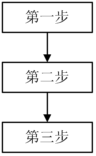
[0030] refer to figure 1 , the manufacturing process of in-mold injection molding circuit, including the following steps:

[0031] The first step, the manufacturing process of the printed circuit film, includes: screen-printing the nano-scale silver paste ink on the matching 0.05-0.25 film to form a printed circuit, and an additional layer can be printed on the printed circuit according to different purposes. insulating ink to form an insulating layer. A hot melt adhesive can also be printed on the insulating layer to form an adhesive layer for integral bonding with the molten plastic under the high temperature conditions of injection molding.

[0032] The second step, the shaping process of the printed circuit film, in...


PUM


Abstract

The invention relates to the technical field of circuit printing technology, in particular to manufacture technology of a printing circuit. The manufacture technology of inlaying an injection circuit in a mold comprises the manufacture technology of a printing circuit film and further comprises film molding integration technology. The printing circuit film is embedded into a mold cavity of an injection mold and formed together with plastics in a molten state in an injection mode, and an integration injection part is manufactured. By the adoption of the technical scheme, the film and plastic gluing technology is once completed in an injection mold. The printed circuit film and a main molding part body are firmly integrated, and the manufacture technology of inlaying the injection circuit in the mold has the advantages that the printed circuit film does not desquamate and not to be oxidated without escaping of small solvent molecules and the like.

Description

technical field [0001] The invention relates to the technical field of circuit printing, in particular to a manufacturing process of a printed circuit. Background technique [0002] At present, the thin-film printed circuit used in the electronics industry is generally bonded with double-sided tape to the main plastic parts. There is a problem of uneven adhesion in this way of bonding. There are local gaps in the film and plastic bonding parts, which are easy to be oxidized and the small molecules of the adhesive solvent are easy to volatilize in the air to cause pollution, which is easy to degumming after a long time. In the production process, there are problems such as high labor cost, low production efficiency, high rejection rate and high production cost. Furthermore, the limitation of the internal space of a large number of micro-appliances makes the operation possibility of bonding the double-sided tape for thin-film printed circuits with the plastic main part very u...

Claims


Application Information

Patent Timeline
Patent Type & Authority Patents(China)
IPC IPC(8): B29C45/14B29C45/17
Inventor 张国庆徐国祥潘永魁
Owner 上海志承新材料有限公司
Why Eureka
Try Eureka