Semiconductor wafer and semiconductor sealing structure

A semiconductor and wafer technology, applied in the field of semiconductor construction, can solve the problems of accelerating crack formation in the metal layer under the bump, reducing the bonding area, shortening the crack growth path, etc.

Inactive Publication Date: 2013-06-19
ADVANCED SEMICON ENG INC
View PDF5 Cites 2 Cited by
  • Summary
  • Abstract
  • Description
  • Claims
  • Application Information

AI Technical Summary

Problems solved by technology

[0004] However, in order to increase the buffer effect, although the opening of the insulating layer can be reduced to increase the buffer area provided by the insulating layer on the pad, this will cause cracks on the connection surface between the UBM layer and the pad. The growth path is shortened, which in turn accelerates the formation of cracks in the metal layer under the bump; and it will reduce the bonding area and reduce the reliability of the connection between the pad and the bump

Method used


Image

  • Semiconductor wafer and semiconductor sealing structure
  • Semiconductor wafer and semiconductor sealing structure
  • Semiconductor wafer and semiconductor sealing structure

Examples


Embodiment Construction

[0017] In order to make the above objects, features and advantages of the present invention more comprehensible, preferred embodiments of the present invention are exemplified below and described in detail in conjunction with the accompanying drawings. Furthermore, the directional terms mentioned in the present invention, such as "up", "down", "front", "back", "left", "right", "inside", "outside", "side", etc., It is only for orientation with reference to the attached drawings. Therefore, the directional terms used are used to illustrate and understand the present invention, but not to limit the present invention.

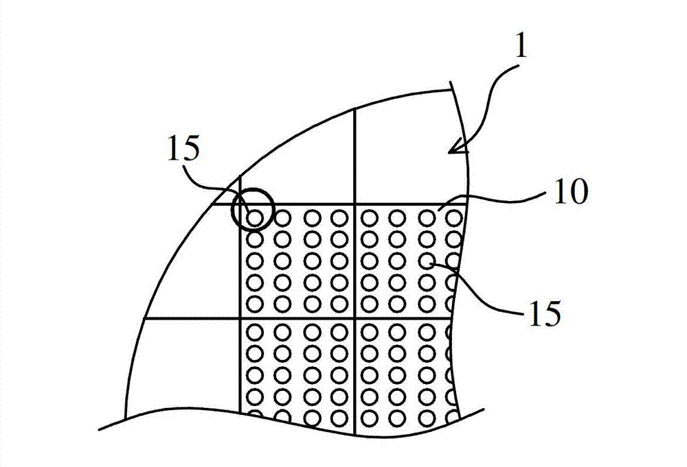
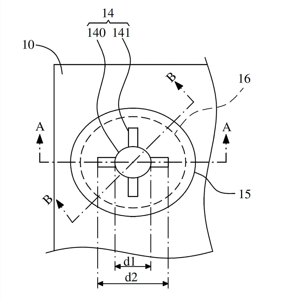
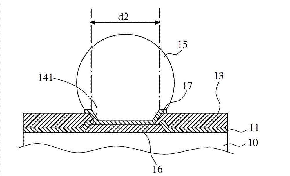
[0018] Please refer to figure 1 , figure 2 , Figure 3A and Figure 3B as shown, figure 1 is a partial top view of a semiconductor wafer according to an embodiment of the present invention; figure 2 yes figure 1 Partial enlarged schematic diagram of ; Figure 3A is along figure 2 Schematic sectional view viewed along line A-A of ; Figure 3B is along ...


PUM


Abstract

The invention discloses a semiconductor wafer and a semiconductor sealing structure. The semiconductor wafer comprises a plurality of chips, an insulating layer, a plurality of protrusion block lower metal layers and a plurality of conduction protrusions. Each chip is provided with an active surface and a plurality of connecting pads formed on the active surface. The insulating layer is formed on the active surfaces of chips and provided with a plurality of opening structures exposing the connecting pads in a corresponding mode. Each opening structure comprises a central opening and at least two extending opening grooves. The hole diameter of each central opening is smaller than the diameter of each connecting pad. Each extending opening groove extends outwards from an edge of each central opening in a radiating mode and keeps a certain distance with the edge of the connecting pad. The plurality of protrusion block lower metal layers are respectively formed on the opening structures and electrically connected with the connecting pads. The plurality of conduction protrusions are respectively formed on the protrusion block lower metal layers. The opening structures of the insulation layer is favorable for enhancing stress buffering effect and increasing combined area of the protrusion block lower metal layers and the connecting pads.

Description

technical field [0001] The invention relates to a semiconductor structure, in particular to a semiconductor wafer with bumps and a semiconductor packaging structure. Background technique [0002] Nowadays, the semiconductor packaging industry has developed various types of packaging structures to meet various demands. In terms of flip chip technology, basically a plurality of conductive bumps are placed on the pads on the active surface of the chip, and then the chip is turned over so that the chip is placed on a substrate through the bumps, and then packaged Adhesive wrapping operation to complete the fabrication of semiconductor packaging structure. [0003] The above process of disposing bumps on the pads on the active surface of the chip can usually be performed directly on the wafer. Generally speaking, an under-bump metallization (UBM) layer is firstly provided on the pad to strengthen the connection between the bump and the pad. The pads on the active surface will ...

Claims


Application Information

Patent Timeline
Patent Type & Authority Applications(China)
IPC IPC(8): H01L23/485
CPCH01L2224/11
Inventor 黄东鸿
Owner ADVANCED SEMICON ENG INC
Why Eureka
Try Eureka