

Display panel and preparation method of packaging structure of display panel
A display panel and packaging structure technology, applied in semiconductor/solid-state device manufacturing, electrical components, electrical solid-state devices, etc., can solve problems such as bubble generation, low moisture permeability, and micro-cracks in the gas barrier layer
- Summary
- Abstract
- Description
- Claims
- Application Information
AI Technical Summary
Problems solved by technology
Method used
Image

Examples
Embodiment Construction
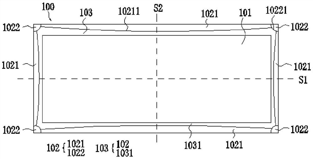
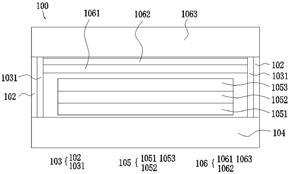
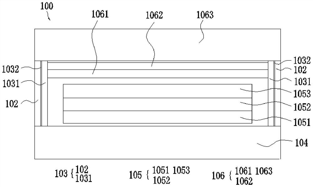
[0029] The following descriptions of the various embodiments refer to the accompanying drawings to illustrate specific embodiments in which the invention may be practiced. The directional terms mentioned in the present invention, such as [top], [bottom], [front], [back], [left], [right], [inside], [outside], [side], etc., are only for reference The orientation of the attached schema. Therefore, the directional terms used are used to illustrate and understand the present invention, but not to limit the present invention. In the figure, units with similar structures are indicated by the same reference numerals, and the dotted lines in the figure indicate that they do not exist in the structure, and only illustrate the shape and position of the structure.
[0030] The present invention aims at the use of adhesives in the prior art to isolate the light-emitting device and the glass substrate from the atmosphere, or to form a gas barrier layer on the substrate by vapor deposition ...
PUM
| Property | Measurement | Unit |
|---|---|---|
| Width | aaaaa | aaaaa |
| Minimum width | aaaaa | aaaaa |
Abstract
Description
Claims
Application Information