Display device and drive method therefor
A technology of a display device and a driving method, which is applied to static indicators, instruments, etc., and can solve the problems of complex circuits and high manufacturing costs
- Summary
- Abstract
- Description
- Claims
- Application Information
AI Technical Summary
Problems solved by technology
Method used
Image

Examples
no. 1 approach
[0128]
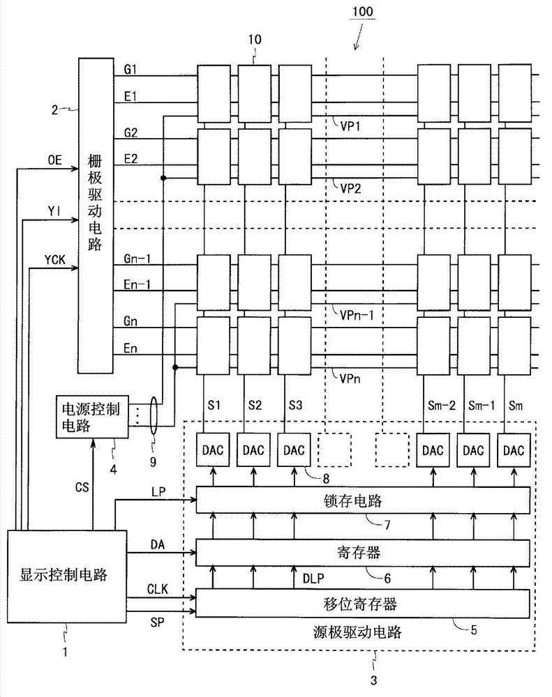
[0129] figure 2 It is a block diagram showing the overall configuration of the display device according to the first embodiment of the present invention. figure 2 The shown display device 100 is an organic EL display including a display control circuit 1 , a gate drive circuit 2 , a source drive circuit 3 , a power supply control circuit 4 , and (m×n) pixel circuits 10 . Hereinafter, let m and n be integers not less than 2, i be an integer not less than 1 and not more than n, and j be an integer not less than 1 and not more than m. In addition, in this embodiment, the row drive circuit is realized by the gate drive circuit 2, and by The source driver circuit 3 realizes a column driver circuit.
[0130] The display device 100 is provided with n scanning signal lines Gi parallel to each other and m data lines Sj parallel to each other and orthogonal thereto. (m×n) pixel circuits 10 are arranged in a matrix corresponding to intersections of scanning signal lines Gi...
no. 2 approach
[0199]
[0200] Figure 13 It is a block diagram showing the overall configuration of the display device according to the second embodiment of the present invention. Figure 13 In the shown display device 200, in addition to the above-mentioned first embodiment (refer to figure 2 ) and further includes a control line drive circuit 20 and a common control line 21 for connecting the control line drive circuit 20 and the control line Ei. In this embodiment, the scanning signal line Gi is connected to the gate drive circuit 2 , and the control line Ei is connected to the control line drive circuit 20 via the common control line 21 . A row drive circuit is realized by the gate drive circuit 2 and the control line drive circuit 20 . In addition, the reason why the control line drive circuit 20 is provided separately from the gate drive circuit 2 is that in this embodiment, as will be described later, each control line Ei is driven, and here the gate drive circuit 2 is used as a...
no. 3 approach
[0228]
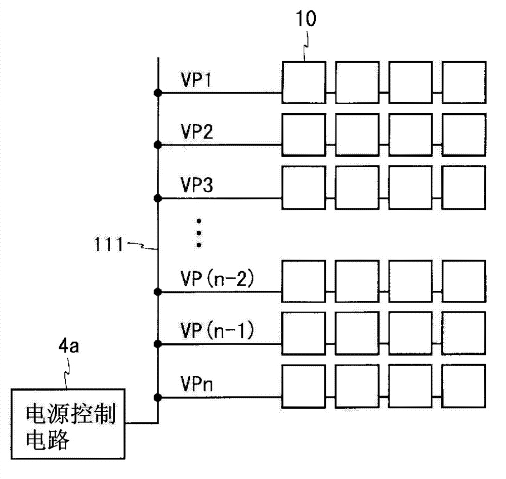
[0229] The overall structure of the display device, the connection method of the power supply line VPi, and the structure of the pixel circuit 10 are the same as those of the above-mentioned first embodiment, so the description thereof will be omitted (see figure 2 , image 3 and Figure 4 ).
[0230]
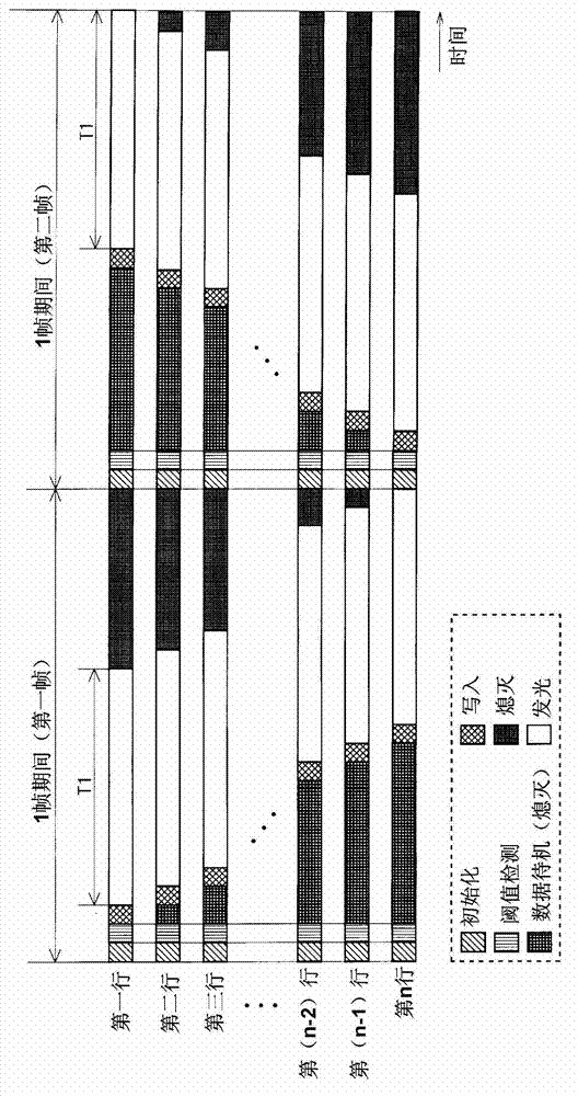
[0231] Figure 24 and Figure 25 It is a timing chart showing a driving method of the pixel circuit 10 of the present embodiment. like Figure 24 and Figure 25 As shown, in this embodiment, regardless of whether it is in the first frame or the second frame, during the period from the end of the threshold value detection of the pixel circuits 10 in all rows to the start of writing in the pixel circuits 10 of each row, The pixel circuits 10 of each row apply a reverse bias (negative bias) to the gate of the TFT 12 (refer to Figure 24 time t14~t15, Figure 25 time t24~t25). The application of the reverse bias voltage to the gate of the TFT 12 is specifical...
PUM
 Abstract
Description
Claims
Application Information
 - R&D
- Intellectual Property
- Life Sciences
- Materials
- Tech Scout
- Unparalleled Data Quality
- Higher Quality Content
- 60% Fewer Hallucinations
Browse by: Latest US Patents, China's latest patents, Technical Efficacy Thesaurus, Application Domain, Technology Topic, Popular Technical Reports.
© 2025 PatSnap. All rights reserved.Legal|Privacy policy|Modern Slavery Act Transparency Statement|Sitemap|About US| Contact US: help@patsnap.com